

Recent development of wide bandgap semiconductor SiC substrates and device
-
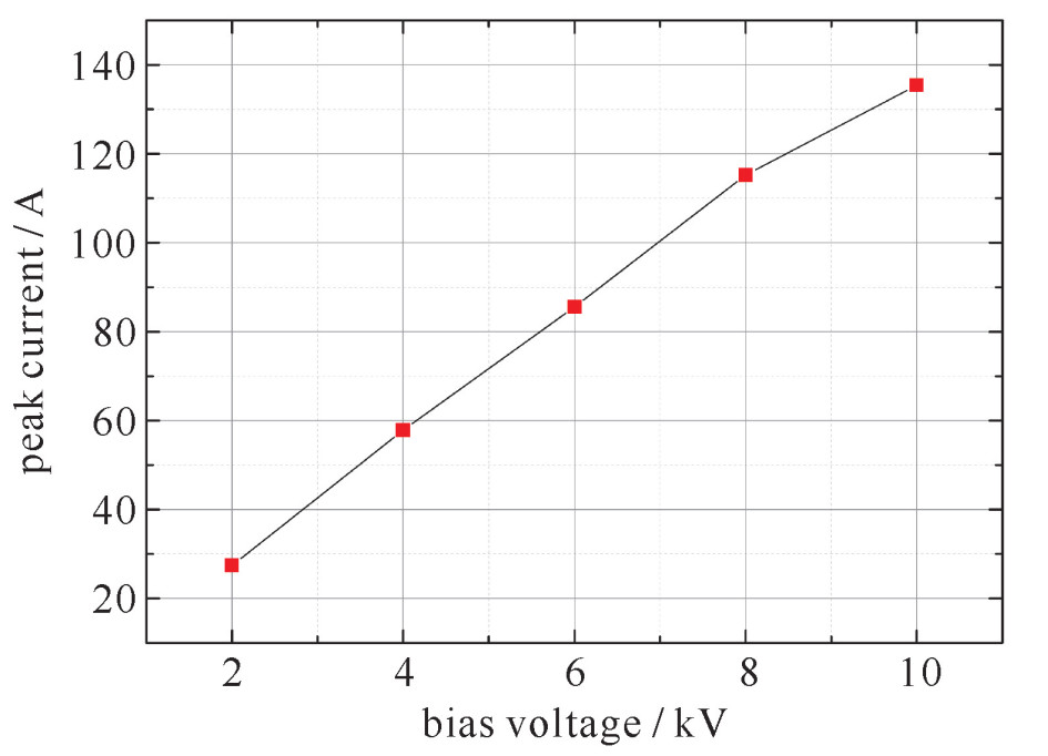
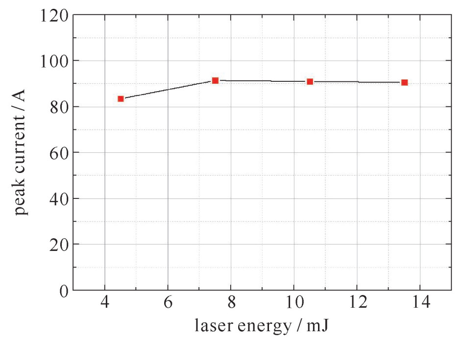
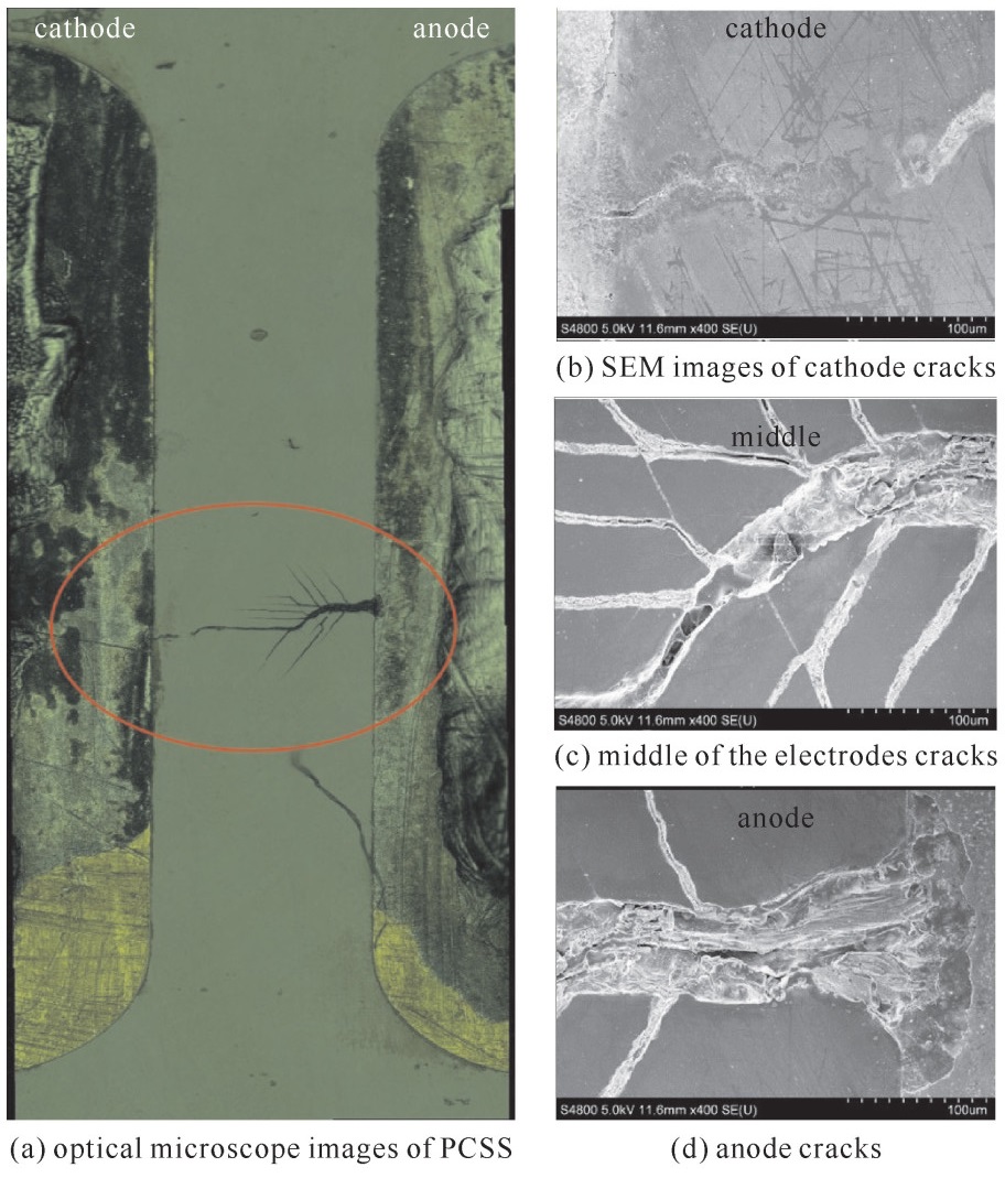
摘要: 碳化硅作为第三代宽禁带半导体的核心材料之一,相对于传统的硅和砷化镓等半导体材料,具有禁带宽度大、载流子饱和迁移速度高,热导率高、临界击穿、场强高等诸多优异的性质。基于这些优良的特性,碳化硅材料是制备高温电子器件、高频大功率器件的理想材料。近年来在碳化硅材料生长和器件制备方面取得重大进展,对碳化硅材料特性和生长方法进行回顾,并研究了碳化硅光导开关偏压、触发能量、导通电流之间的关系,以及开关失效情况下电极表面的损伤情况。Abstract: As a key representative material for the third-generation wide bandgap semiconductors, silicon carbide (SiC) is a promising wide band gap semiconductor material and can be used for the fabrication of high-power and high-frequency electronics, due to its superior physical properties, such as high thermal conductivity, wide band gap and high critical breakdown field. In recent years, bulk growth of SiC single crystals and the fabrication of devices have made significant progress. The paper introduces the growth techniques for SiC bulk and presents the relationship between the on-state resistance and voltage or laser energy. It also analyses the failure of devices.
-
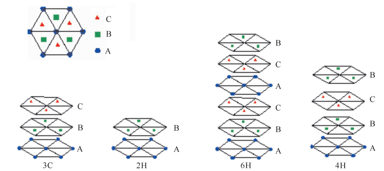
图 1 不同构型的SiC单晶的硅碳双原子层排列顺序
Figure 1. Stacking sequence of double atomic layers of different SiC polytypes
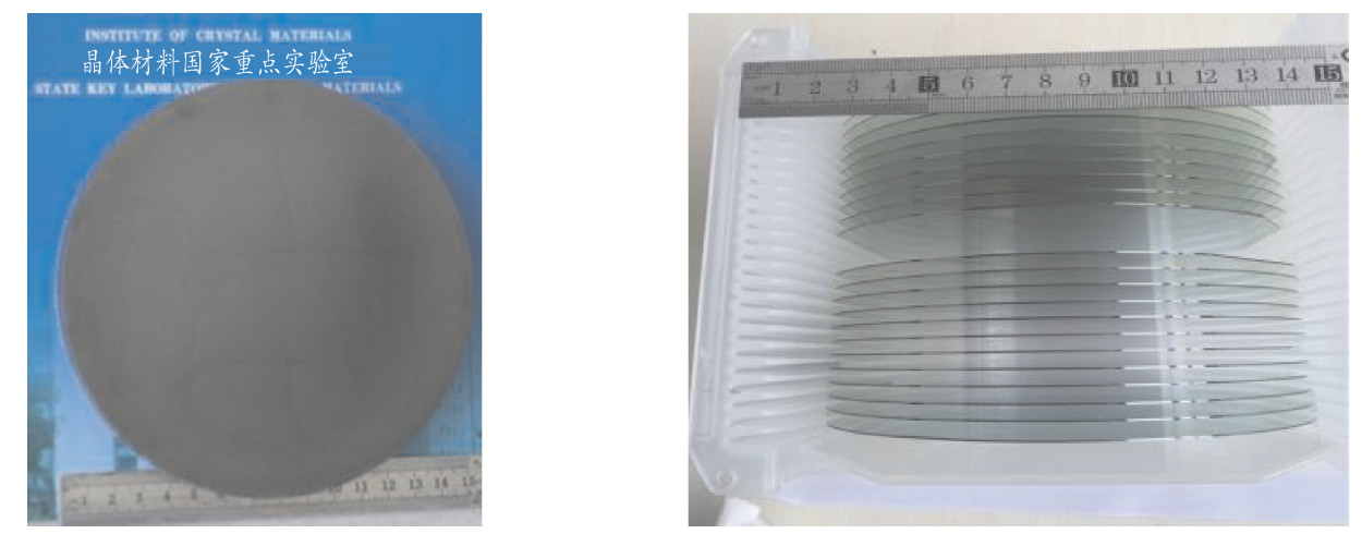
图 4 山东大学6 inch SiC单晶及衬底
Figure 4. 6 inch SiC single crystal and substrate grown by Shandong University
表 1 SiC与Si和GaAs的物理特性参数比较
Table 1. Properties comparison between Si, GaAs and SiC
material band gap/eV dielectric constant breakdown field/(MV·cm-1) saturated electron drift velocity/(cm·s-1) intrinsic carrier concentration/cm-3 electron mobility/(cm2·V·s-1) thermal conductivity/(W·cm-1·K-1) Si 1.12 11.8 0.3 1.0×10⁷ 1.5×10¹⁰ 1400 1.50 GaAs 1.43 12.8 0.6 1.0×10⁷ 1.8×10⁶ 8500 0.46 6H-SiC 3.03 9.6 3.2 2.0×10⁷ 2.3×10⁻⁶ 400 4.90 4H-SiC 3.26 9.7 3.0 2.0×10⁷ 8.2×10⁻⁹ 1140 4.90  下载: 导出CSV
-
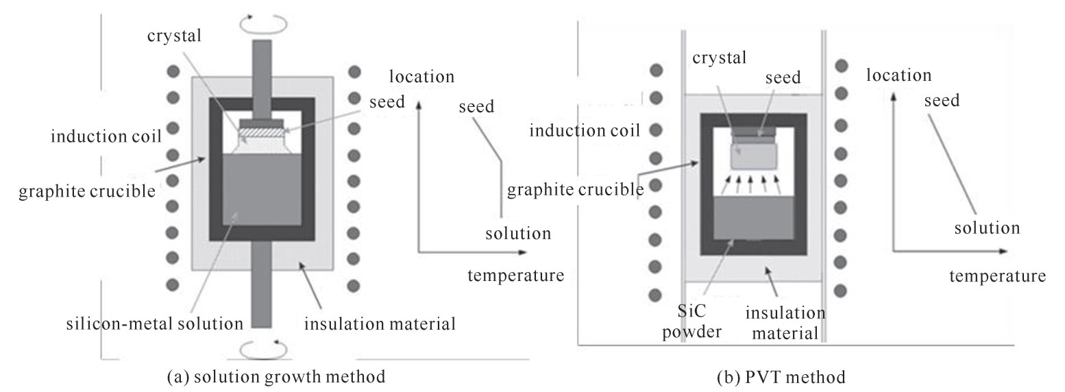
[1] Powell A R, Rowland L B. SiC materials—progress, status, and potential roadblocks[J]. Proceedings of the IEEE, 2002, 90(6): 942-955. doi: 10.1109/JPROC.2002.1021560 [2] Neudeck P G, Okojie R S, Chen L Y. High temperature electronics—a role for wide bandgap semiconductors[J]. Proc of the IEEE, 2006, 90(6): 1065-1076. [3] Hudgins J. Wide and narrow bandgap semiconductors for power electronics: A new valuation[J]. Journal of Electronic Material, 2003, 32(6): 471-477. doi: 10.1007/s11664-003-0128-9 [4] Morkoc H, Strite S, Gao G B, et al. Large-band-gap SiC, Ⅲ-V nitride, and Ⅱ-VI ZnSe-based semiconductor device technologies[J]. Journal of Applied Physics, 1994, 76(3): 1363-1398. doi: 10.1063/1.358463 [5] 郝跃, 彭军, 杨银堂. 碳化硅宽带隙半导体技术[M]. 北京: 科学出版社, 2000: 116-119.Hao Yue, Peng Jun, Yang Yintang. The technology of silicon carbide broadband gap semiconductor. Beijing: Science Press, 2000: 116-119 [6] Glass R C, Henshall D, Tsvetkov V F, et al. SiC-seeded crystal growth[J]. MRS Bulletin, 1997, 22(3): 30-35. doi: 10.1557/S0883769400032735 [7] Yashiro N, Kusunoki K, Kamei K, et al. Growth of SiC single crystal from Si-C-(Co, Fe) ternary solution[C]//Materials science forum. Trans Tech Publications, 2006, 527: 115-118. [8] Kimoto T, Cooper J A. Fundamentals of silicon carbide technology: growth, characterization, devices and applications[M]. John Wiley & Sons, 2014. [9] Danno K, Saitoh H, Seki A, et al. High-speed growth of high-quality 4H-SiC bulk by solution growth using Si-Cr based melt[J]. Materials Science Forum, 2010, 645/648: 13-16. doi: 10.4028/www.scientific.net/MSF.645-648.13 [10] 彭燕, 陈秀芳, 彭娟, 等. 高质量半绝缘ϕ150 mm 4H-SiC单晶生长研究[J]. 人工晶体学报, 2016, 45(5): 1145-1152. doi: 10.3969/j.issn.1000-985X.2016.05.001Peng Yan, Chen Xiufang, Peng Juan, et al. Study on the growth of high quality semi-insulating ϕ150 mm 4H-SiC single crystal. Journal of Synthetic Crystals, 2016, 45(5): 1145-1152 doi: 10.3969/j.issn.1000-985X.2016.05.001 [11] Bluhm H. Pulsed power systems[M]. Berlin: Springer-Verlag, 2006. [12] Cho P S, Goldhar J, Lee C H, et al. Photoconductive and photovoltaic response of high-dark-resistivity 6H-SiC devices[J]. Journal of Applied Physics, 1995, 77(4): 1591-1599. doi: 10.1063/1.358912 [13] Sheng S, Spencer M G, Tang X, et al. Polycrystalline cubic silicon carbide photoconductive switch[J]. IEEE Electron Device Lett, 1997, 18(8): 372-374. doi: 10.1109/55.605443 [14] Dogˇ an S, Teke A, Huang D, et al. 4H-SiC photoconductive switching devices for use in high-power applications[J]. Applied Physics Letters, 2003, 82(18): 3107-3109. doi: 10.1063/1.1571667 [15] Zhu K, Dogˇ an S, Moon Y T, et al. Effect of n+-GaN subcontact layer on 4H-SiC high-power photoconductive switch[J]. Applied Physics Letters, 2005, 86: 261108. doi: 10.1063/1.1951056 [16] Mauch D, Sullivan W, Bullick A, et al. High power lateral silicon carbide photoconductive semiconductor switches and investigation of degradation mechanisms[J]. IEEE Trans Plasma Science, 2015, 43(6): 2021-2031. doi: 10.1109/TPS.2015.2424154 [17] Tiskumara R, Joshi R P, Mauch D, et al. Analysis of high field effects on the steady-state current-voltage response of semi-insulating 4H-SiC for photoconductive switch applications[J]. Journal of Applied Physics, 2015, 118: 095701. doi: 10.1063/1.4929809 [18] Chowdhury A R, Mauch D, Joshi R P, et al. Contact extensions over a high-dielectric layer for surface field mitigation in high power 4H-SiC photoconductive switches[J]. IEEE Trans Electron Devices, 2016, 63(8): 3171-3176. [19] 刘金锋, 袁建强, 刘宏伟, 等. 影响碳化硅光导开关最小导通电阻的因素[J]. 强激光与粒子束, 2012, 24(3): 607-611. doi: 10.3788/HPLPB20122403.0607Liu Jinfeng, Yuan Jianqiang, Liu Hongwei, et al. Factors affecting minimum on-state resistance of SiC photoconductive semiconductor switch. High Power Laser and Particle Beams, 2012, 24(3): 607-611 doi: 10.3788/HPLPB20122403.0607 [20] 周天宇, 刘学超, 代冲冲, 等. V掺杂6H-SiC光导开关制备与性能研究[J]. 强激光与粒子束, 2014, 26: 045043. doi: 10.11884/HPLPB201426.045043Zhou Tianyu, Liu Xuechao, Dai Chongchong, et al. Fabrication and properties of V-doped semi-insulating 6H-SiC photoconductive semiconductor switch. High Power Laser and Particle Beams, 2014, 26: 045043 doi: 10.11884/HPLPB201426.045043 [21] Cao Penghui, Huang Wei, Guo Hui, et al. Performance of a vertical 4H-SiC photoconductive switch with AZO transparent conductive window and silver mirror reflector[J]. IEEE Trans Electron Devices, 2018, 65(5): 2047-2051. doi: 10.1109/TED.2018.2815634 [22] Xiao Longfei, Yang Xianglong, Duan Peng, et al. Effect of electron avalanche breakdown on a high-purity semi-insulating 4H-SiC photoconductive semiconductor switch under intrinsic absorption[J]. Applied Optics, 2018, 57(11): 2804-2808. doi: 10.1364/AO.57.002804 [23] Luan Chongbiao, Li Boting, Zhao Juan, et al. A new phenomenon in semi-insulating 4H-SiC photoconductive semiconductor switches[J]. IEEE Trans Electron Devices, 2018, 65(1): 172-175. doi: 10.1109/TED.2017.2777600 -


 点击查看大图
图(8) / 表(1)
计量
- 文章访问数: 1936
- HTML全文浏览量: 388
- PDF下载量: 364
- 被引次数: 0
