

Patterning of graphene by light field modulated nanosecond laser
-
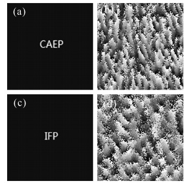
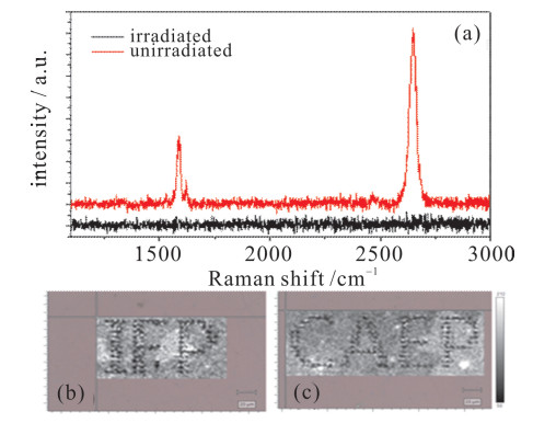
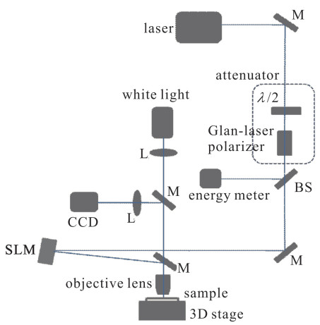
摘要: 激光加工技术在石墨烯制备领域得到了许多应用。目前激光图案化石墨烯的方法多为激光逐点扫描, 而单次辐照实现图案化加工的方法鲜有报道。通过间光调制器改变激光的光场, 使光束聚焦成图案, 单次辐照直接在石墨烯样品上烧蚀实现图案化。控制激光能量为合适的值时可将石墨烯清晰地图案化而不损伤硅基底。通过拉曼光谱扫描成像发现石墨烯加工边缘清晰, 精度达到μm量级, 具有加工速度快、无需移动样品等特点。Abstract: Laser-based approaches for graphene synthesis, reduction, modification, cutting and micro-patterning have been developed and applied to the fabrication of various electronic devices.General method utilized in direct laser writing and patterning of graphene was realized by controlling the movement of the sample or the laser reflecting mirror, while patterning by single shot laser is rarely reported.In the present study, a single shot laser patterning graphene method via light field modulating is proposed.Via controlling the light field by special light modulator (SLM), nanosecond laser pulses focused by objective lens were modulated to the desired pattern.The 4layer graphene in the laser irradiate region was damaged when laser energy was lager than 0.03 mJ.When the laser energy reached 0.06 mJ, clear pattern formed in graphene while no damage occurred in silicon base.The characteristics of graphene patterns were measured using Raman spectra imaging technology.The experimental results revealed that the light field modulated nanosecond laser remains potentially advantageous in graphene micro pattern processing with no need of moving the sample, quick processing and micrometer precision.
-
Key words:
- graphene /
- laser /
- Raman spectra /
- laser processing /
- patterning
-
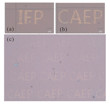
图 3 单脉冲纳秒激光加工的石墨烯图案
Figure 3. Graphene patterns processed by single shot nanosecond laser
-
[1] Novoselov K S, Geim A K, Morozov S V, et al. Electric field effect in atomically thin carbon films[J]. Science, 2004, 306(22): 666-669. [2] Morozov S V, Novoselov K S, Katsnelson M I, et al. Giant intrinsic carrier mobilities in graphene and its bilayer[J]. Phys Rev Lett, 2008, 100: 016602. doi: 10.1103/PhysRevLett.100.016602 [3] Nair R R, Blake P, Grigorenko A N, et al. Fine structure constant defines visual transparency of graphene[J]. Science, 2008, 321(6): 1308. [4] Lee C, Wei X, Kysar J W, et al. Measurement of the elastic properties and intrinsic strength of monolayer graphene[J]. Science, 2008, 321(18): 385-388. [5] Krauss B, Lohmann T, Chae D H, et al. Laser-induced disassembly of a graphene single crystal into a nanocrystalline network[J]. Phys Rev B, 2009, 79: 165428. doi: 10.1103/PhysRevB.79.165428 [6] Qian M, Zhou Y S, Gao Y, et al. Formation of graphene sheets through laser exfoliation of highly ordered pyrolytic graphite[J]. Appl Phys Lett, 2011, 98: 173108. doi: 10.1063/1.3584021 [7] Lee S, Toney M F, Ko W, et al. Laser-synthesized epitaxial graphene[J]. ACS Nano, 2010, 4(12): 7524-7530. doi: 10.1021/nn101796e [8] Park J B, Xiong W, Gao Y, et al. Fast growth of graphene patterns by laser direct writing[J]. Appl Phys Lett, 2011, 98: 123109. doi: 10.1063/1.3569720 [9] Huang L, Liu Y, Ji L C, et al. Pulsed laser assisted reduction of graphene oxide[J]. Carbon, 2011, 49(7): 2431-2436. doi: 10.1016/j.carbon.2011.01.067 [10] Roberts A, Cormode D, Reynolds C, et al. Response of graphene to femtosecond high-intensity laser irradiation[J]. Appl Phys Lett, 2011, 99: 051912. doi: 10.1063/1.3623760 [11] Zhou Y, Bao Q L, Varghese B N, et al. Microstructuring of graphene oxide nanosheets using direct laser writing[J]. Adv Mater, 2010, 22(1): 67-71. doi: 10.1002/adma.200901942 [12] 吴凌远, 李阳龙, 刘国栋, 等. 1064 nm纳秒激光对石墨烯的损伤效应研究[J]. 强激光与粒子束, 2015, 27: 081009. doi: 10.11884/HPLPB201527.081009Wu Lingyuan, Li Yanglong, Liu Guodong, et al. 1064 nm nanosecond laser induced damage effect on graphene. High Power Laser and Particle Beams, 2015, 27: 081009 doi: 10.11884/HPLPB201527.081009 [13] Jani K, Christian B, Yigal L, et al. Toward two-dimensional all-carbon heterostructures via ion beam patterning of single-layer graphene[J]. Nano Lett, 2015, 15(9): 5944-5949. doi: 10.1021/acs.nanolett.5b02063 [14] Chen Y, Zhang N, Li Y F, et al. Microscal E-patterned graphene electrodes for organic light-emitting devices by a simple patterning strategy[J]. Adv Optical Mater, 2018, 13: 1701348. [15] Ethan B S, Pradyumna L P, Kanan P, et al. Inkjet printing of high conductivity, flexible graphene patterns[J]. J Phys Chem Lett, 2013, 4(8): 1347-1351. doi: 10.1021/jz400644c [16] 南洋, 张建寰, 张陈涛. 激光直写制备石墨烯研究进展[J]. 化工新型材料, 2015, 43(12): 1-3. https://www.cnki.com.cn/Article/CJFDTOTAL-HGXC201512001.htmNan Yang, Zhang Jianhuan, Zhang Chentao. Progress in laser direct writing synthesis of graphene. New Chemical Materials. 2015, 43(12): 1-3 https://www.cnki.com.cn/Article/CJFDTOTAL-HGXC201512001.htm [17] Chen H Y, Han D D, Tian Y, et al. Mask-free and programmable patterning of graphene by ultrafast laserdirect writing[J]. Chemical Physics, 2014, 430: 13-17. doi: 10.1016/j.chemphys.2013.12.005 [18] Chang T L, Chen Z C, Chen W Y, et al. Patterning of multilayer graphene on glass substrate by using ultraviolet picosecond laser pulses[J]. Microelectronic Engineering, 2016, 158(1): 1-5. [19] Lee K, Ki H. Fabrication and optimization of transparent conductive films using laser annealing and picosecond laser patterning[J]. Applied Surface Science, 2017, 420(1): 886-895. [20] Pechlivani E M, Papas D, Mekeridis C, et al. Ultra-short pulse laser for patterning high quality graphene electrodes[J]. Materials Today: Proceedings, 2017, 4(4): 5074-5081. doi: 10.1016/j.matpr.2017.04.116 [21] Kumar R, Singh R K, Singh D P, et al. Laser-assisted synthesis, reduction and micro-patterning of graphene: Recent progress and applications[J]. Coordination Chemistry Reviews, 2017, 342: 34-79. doi: 10.1016/j.ccr.2017.03.021 -

 下载:
下载:
 点击查看大图
图(4)
计量
- 文章访问数: 1159
- HTML全文浏览量: 279
- PDF下载量: 87
- 被引次数: 0
