

Failure mechanism of a kind of FPGA chip under RF interference
-
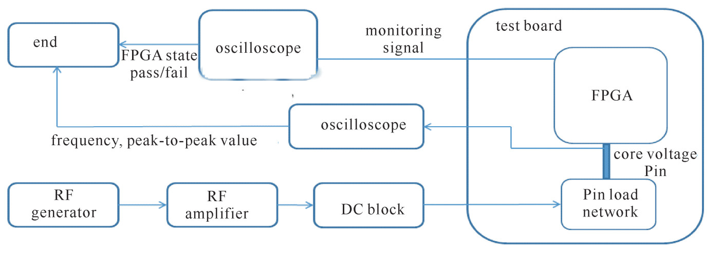
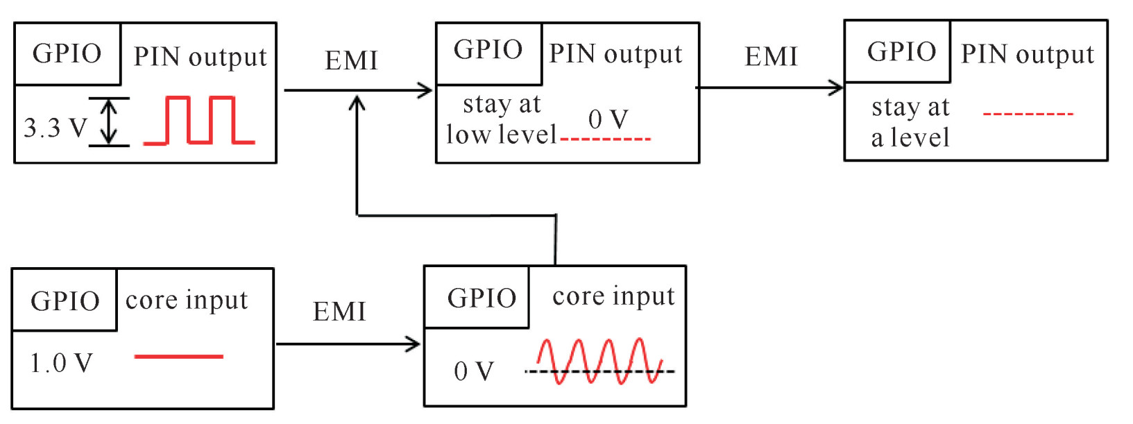
摘要: 研究了一种Xilinx公司FPGA芯片XC7A200T-2FBG676在射频干扰下的失效机理。通过对该FPGA内核供电引脚注入射频干扰发现,某些频率下,随着干扰强度的增大,FPGA会依次出现三种不同类型的失效,分别为该FPGA的内核失效、I/O失效和配置失效。测试分析和HSPICE仿真表明,内核失效是由于BRAM的逻辑层抗扰性差所致,I/O失效是由于射频干扰下输入/输出信号的同时失真所致,配置失效则是由于配置系统读取错误的配置使能信号所致。研究可为该FPGA芯片或者系统电磁兼容设计以及该FPGA抗扰性检测方案的制定提供指导。Abstract: The failure mechanism of Xilinx's FPGA chip XC7A200T-2FBG676 under RF interference is studied. When RF interference injects into the power supply pins of the FPGA core, it is found that with the increase of interference intensity at the some frequencies, three types of FPGA failures occur successively, namely core failure, I/O failure and configuration failure. Test analysis and HSPICE simulation show that the core failure is due to the poor disturbance immunity of the logic layer of BRAM, the I/O failure is due to the simultaneous distortion of input/output signals under RF interference, and the configuration failure is due to the configuration system reading the wrong configuration enable signal. This study could provide guidance for the electromagnetic compatibility design of this kind of FPGA chip or system, as well as the formulation of electromagnetic immunity detection scheme of this kind of FPGA.
-
Key words:
- FPGA /
- radio-frequency interference /
- FPGA core /
- FPGA failure
-
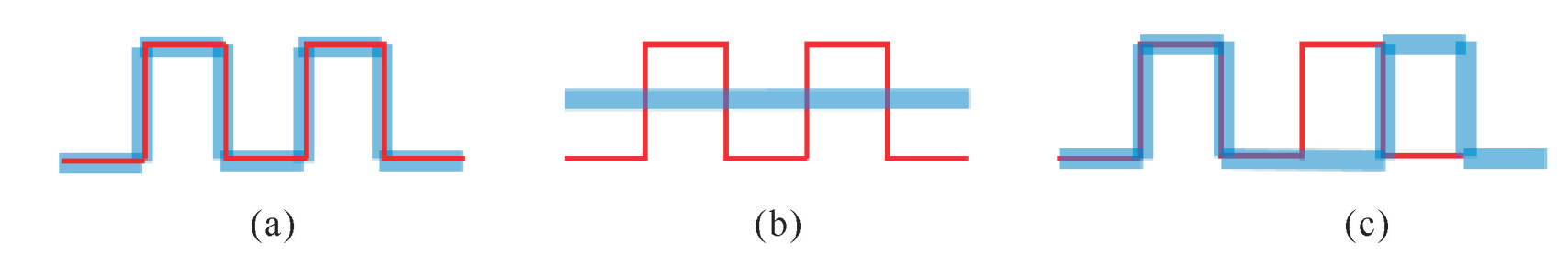
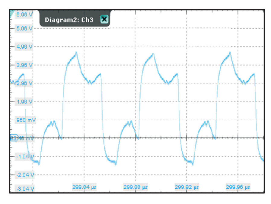
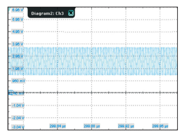
图 1 反馈信号在EMI下的变化:正常情况(a),电平失配(b)和周期失配(c)
Figure 1. Change of feedback signal under EMI: normal state(a), level mismatch(b) and cycle mismatch(c)
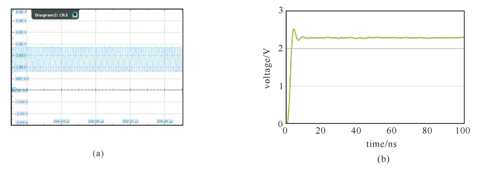
图 7 I/O失效时反馈信号特征(a)和其滤波后特征(b)
Figure 7. Feedback signal feature (a) and its filtered feature (b) when I/O fails
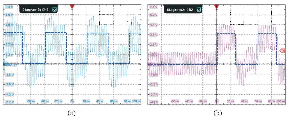
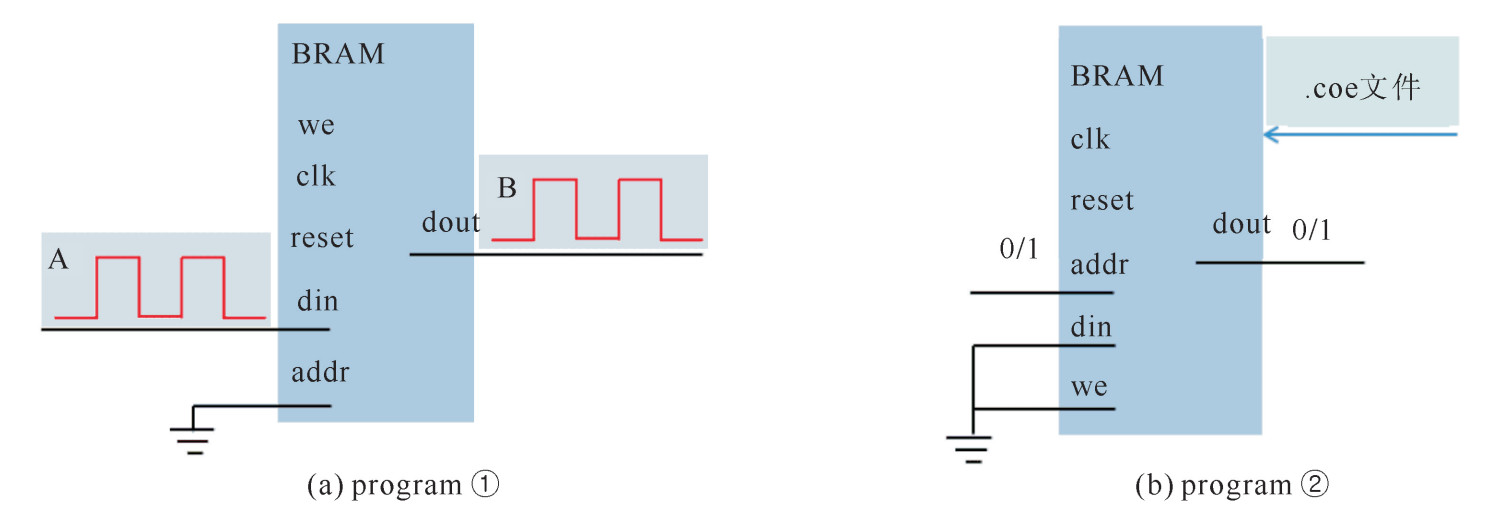
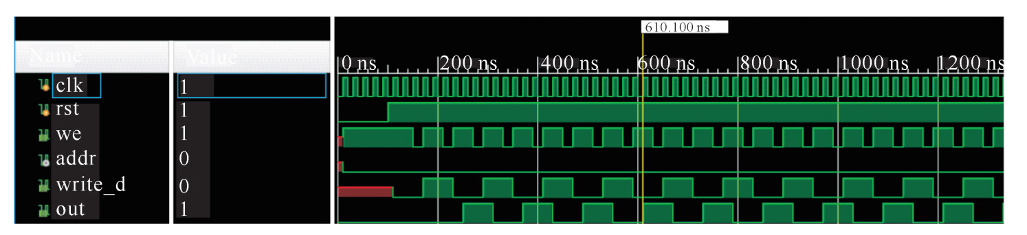
图 9 内核失效时反馈信号(a)和BRAM输出特征图(b)
Figure 9. Feedback signal feature (a) and BRAM output feature (b) when core fails
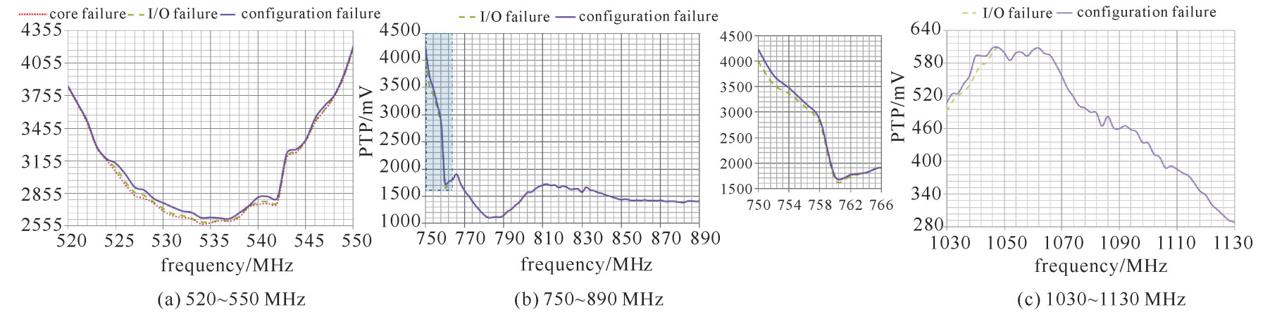
图 10 FPGA失效曲线图
Figure 10. FPGA failure curves: 520 MHz~550 MHz(a), 750 MHz~890 MHz(b) and 1030 MHz~1130 MHz(c)
-
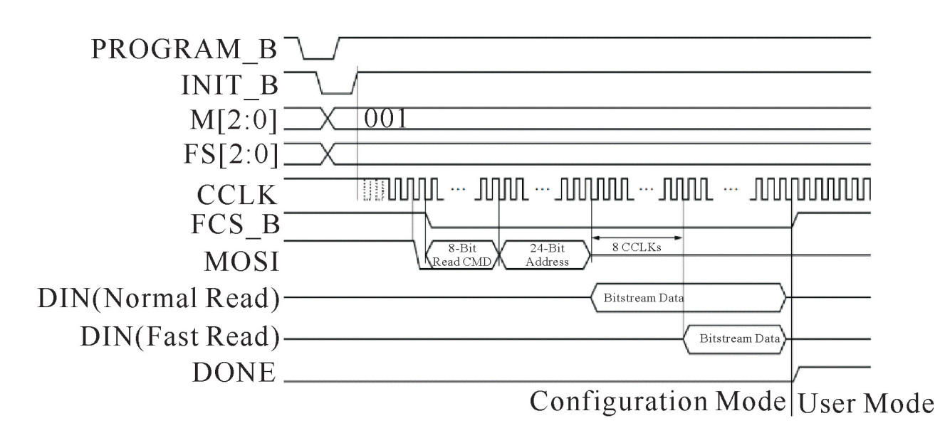
[1] Christopoulos C. Electromagnetic compatibility (EMC) in challenging environments[M]. Springer International Publishing, 2017. [2] 黎明, 黄如. 后摩尔时代大规模集成电路器件与集成技术[J]. 中国科学: 信息科学, 2018, 48(8): 963-977. https://www.cnki.com.cn/Article/CJFDTOTAL-PZKX201808001.htmLi Ming, Huang Ru. Device and integration technologies for VLSI in post-Moore era. Scientia Sinica: Informationis, 2018, 48(8): 963-977 https://www.cnki.com.cn/Article/CJFDTOTAL-PZKX201808001.htm [3] Coulson D R. EMC-hardening microprocessor-based systems[C]//IEE Colloquium on Achieving Electromagnetic Compatibility: Accident or Design. 1997. [4] Fiori F, Musolino F. Analysis of EME produced by a microcontroller operation[C]//Proceedings Design, Automation and Test in Europe Conference and Exhibition. 2001. [5] Su T, Unger M, Steinecke T, et al. Using Error-Source Switching (ESS) concept to analyze the conducted radio frequency electromagnetic immunity of microcontrollers[J]. IEEE Transactions on Electromagnetic Compatibility, 2012, 54(3): 634-645. doi: 10.1109/TEMC.2011.2165341 [6] Dehbaoui A, Dutertre J M, Robisson B, et al. Electromagnetic transient faults injection on a hardware and a software implementations of AES[C]//Fault Diagnosis and Tolerance in Cryptography (FDTC). 2012. [7] Zussa L, Dehbaoui A, Tobich K, et al. Efficiency of a glitch detector against electromagnetic fault injection[C]//Conference on European Design and Automation Association. 2014. [8] Ren L, Li T, Chandra S. Prediction of power supply noise from switching activity in an FPGA[J]. IEEE Transactions on Electromagnetic Compatibility, 2014, 56(3): 699-706. doi: 10.1109/TEMC.2013.2293872 [9] 程俊平, 周长林, 余道杰, 等. 基于供电网络传导耦合的FPGA电磁敏感特性分析[J]. 强激光与粒子束, 2019, 31: 023202. doi: 10.11884/HPLPB201931.180322Cheng Junping, Zhou Changlin, Yu Daojie, et al. Electromagnetic susceptibility analysis of FPGA based on conducted coupling of power supply network. High Power Laser and Particle Beams, 2019, 31: 023202 doi: 10.11884/HPLPB201931.180322 [10] Xilinx Inc. Series FPGAs Configuration User Guide. Version[EB/OL]. http://china.xilinx.com/support/documentation/user_guides/ug470_7Series_Config.pdf. -

 下载:
下载:
 点击查看大图
计量
- 文章访问数: 1966
- HTML全文浏览量: 573
- PDF下载量: 80
- 被引次数: 0
