

Influence of surface sand blasting treatment on vacuum surface flashover characteristics of PMMA insulator
-
摘要: 绝缘子表面粗糙处理是提升其沿面闪络性能的重要途径,表面粗糙化处理方式不当,极易带来表面结构不均匀,难以获得稳定耐压性能的绝缘材料。为提升绝缘子表面粗糙处理的均匀性,本文利用表面喷砂技术对圆柱形有机玻璃(PMMA)绝缘子进行了粗糙化处理研究,以球形二氧化硅(SiO2)颗粒为工作介质,研究了不同喷砂粒径、氢氟酸后处理等因素对绝缘材料表面形貌和组分的影响,并利用短脉冲高压测试平台对喷砂处理前后有机玻璃绝缘子样品进行了真空沿面闪络性能测试。研究结果表明,喷砂处理在有机玻璃表面形成了较为均匀的凹坑,HF酸能够有效去除表面残留的SiO2颗粒,具有表面喷砂粗糙结构的绝缘子沿面闪络电压得到了稳定提升,相较于未处理的绝缘子闪络电压提升了约80%。Abstract: Surface roughening treatment on insulators is an important way to improve their vacuum surface flashover characteristics. However, flashover voltages of the insulators with the same roughness show big deviation because of the poor uniformity of the surface rough structure and bad repeatability of the surface roughening method. To improve the uniformity of the surface roughening and the stability of the voltage-withstanding of the vacuum insulators, sand blasting roughening treatment on the surface of the cylindrical PMMA insulators was studied. First of all, the cylindrical insulators were sprayed on the rotating platform. With the collisions of the spherical micro SiO2 particles carried by the high-speed airflow, rough structure was fabricated on the surface. After the corrosion of the HF acid, residual SiO2 particles were removed, leaving homogeneous rough structure on the surface. The changes of the surface morphology were studied by Scanning Electron Microscope and the surface roughness of the treated insulators was tested on the surface roughness meter. Surface flashover characteristics of the sand-sprayed PMMA specimens were tested on the short-pulsed high-voltage platform. The test results indicated that homogeneously rough surface was prepared by the sand blasting treatment and the surface flashover voltages of the treated insulators were improved steadily. Compared with the untreated PMMA specimens, flashover voltages of the sand blasted insulators were improved approximately 80%.
-
Key words:
- surface flashover /
- PMMA /
- sand blasting treatment /
- surface roughness
-
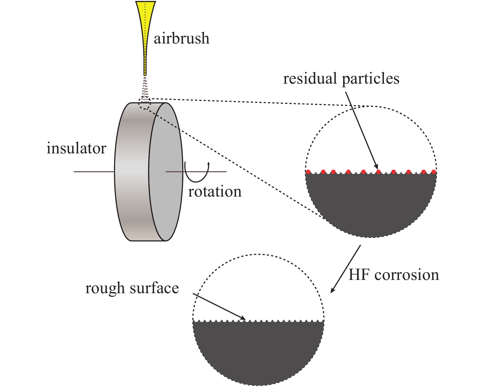
图 2 绝缘子表面旋转喷砂处理过程示意图
Figure 2. Schematic of the rotating sand blasting process on the surface of the insulators
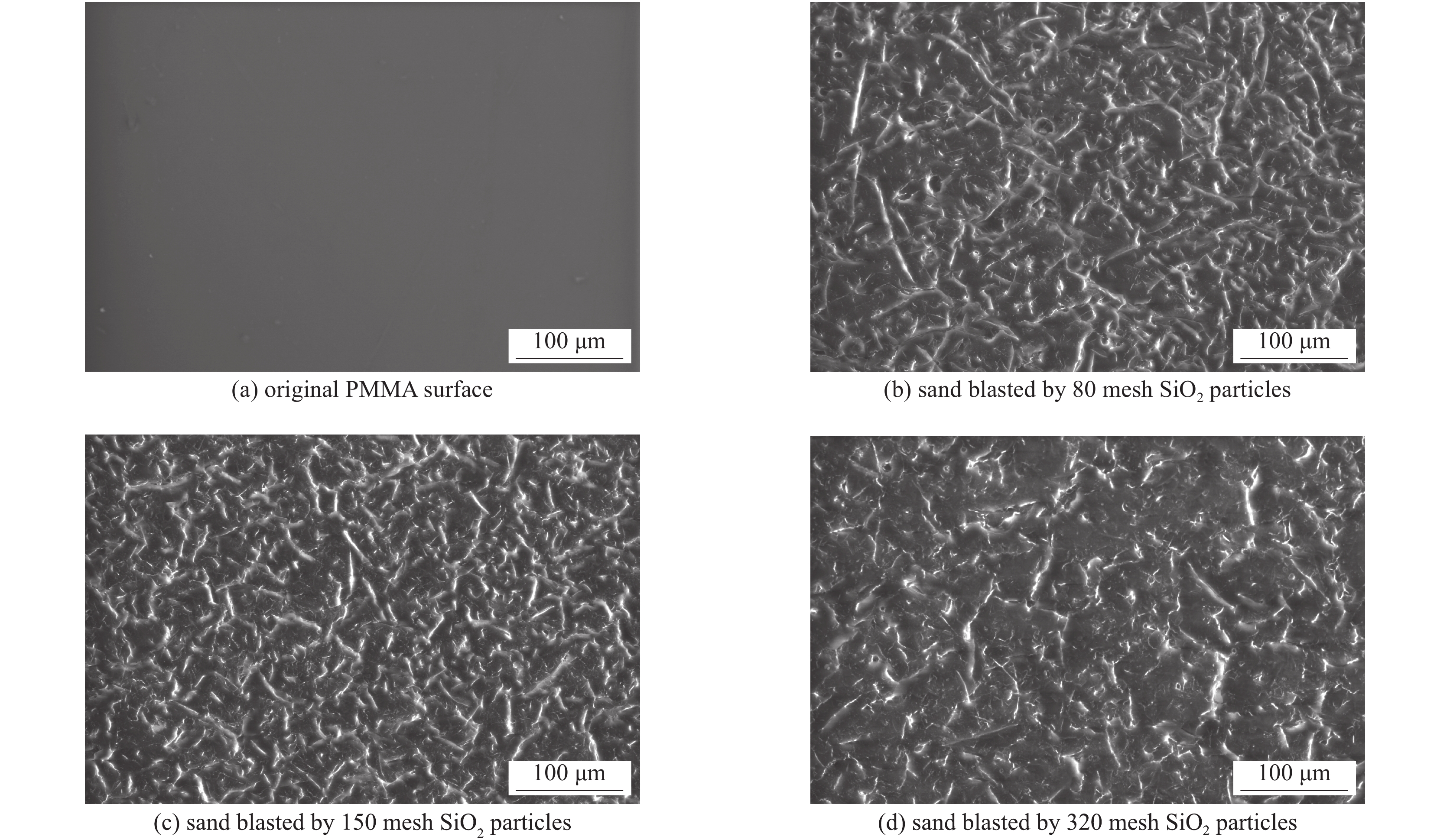
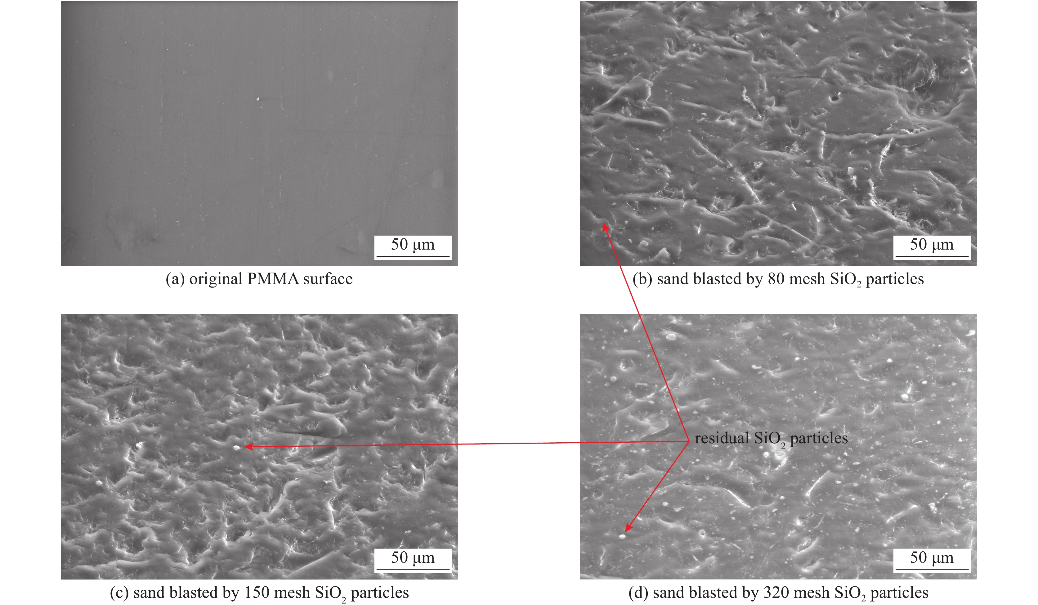
图 4 喷砂处理样品HF酸处理后表面形貌变化
Figure 4. Changes of the surface morphology after sand blasting and HF acid corrosion
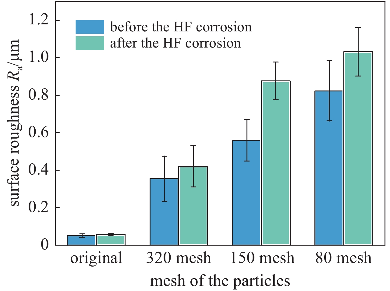
图 5 表面喷砂处理及HF酸腐蚀对绝缘子表面粗糙度的影响
Figure 5. Influence of the sand blasting and HF acid corrosion on the surface roughness
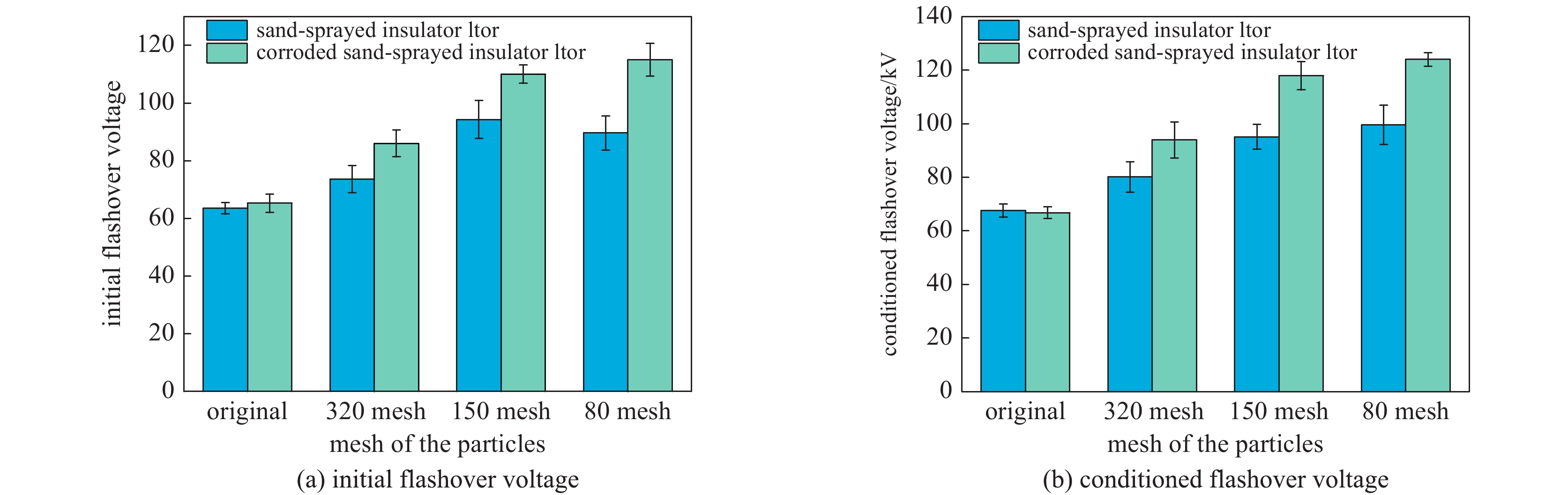
图 6 表面喷砂处理及HF酸腐蚀对绝缘子沿面闪络的影响
Figure 6. Influence of the sand blasting and HF acid corrosion on the flashover voltages of the insulators
表 1 样品处理后表面粗糙度
Table 1. Surface roughness of the treated specimens
treatment roughness/μm original 320 meshes 150 meshes 80 meshes without HF corrosion 0.051 0.355 0.559 0.822 with HF corrosion 0.056 0.421 0.876 1.031  下载: 导出CSV
-
[1] Li S, Nie Y, Min D, et al. Research progress on vacuum surface flashover of solid dielectrics[J]. Transactions of China Electrotechnical Society, 2017, 32(8): 1-9. [2] Miller H C. Flashover of insulators in vacuum: The last twenty years[J]. IEEE Trans Dielectrics & Electrical Insulation, 2016, 22(6): 3641-3657. [3] Miller H C. Surface flashover of insulators[J]. IEEE Trans Electrical Insulation, 1989, 24(5): 765-786. doi: 10.1109/14.42158 [4] Pillai A S, Hackam R. Surface flashover of solid insulators in atmospheric air and in vacuum[J]. Journal of Applied Physics, 1985, 58(1): 146-153. [5] Li C, Hu J, Lin C, et al. Surface charge migration and dc surface flashover of surface-modified epoxy-based insulators[J]. Journal of Physics D Applied Physics, 2017, 50: 065301. doi: 10.1088/1361-6463/aa5207 [6] Huo Y, Liu W, Ke C, et al. Sharp improvement of flashover strength from composite micro-textured surfaces[J]. Journal of Applied Physics, 2017, 122: 115105. doi: 10.1063/1.4991934 [7] Shao T, Zhou Y, Zhang C, et al. Surface modification of polymethyl-methacrylate using atmospheric pressure argon plasma jets to improve surface flashover performance in vacuum[J]. IEEE Trans Dielectrics & Electrical Insulation, 2015, 22(3): 1747-1754. [8] Cai L, Wang J, Cheng G, et al. Simulation of multipactor on the rectangular grooved dielectric surface[J]. Physics of Plasmas, 2015, 22: 113506. doi: 10.1063/1.4935385 [9] 李逢, 王勐, 任靖, 等. 不同微槽结构绝缘子真空沿面闪络特性[J]. 强激光与粒子束, 2014, 26:045049. (Li Feng, Wang Meng, Ren Jing, et al. Characteristics of grooved insulator flashover under pulsed voltage[J]. High Power Laser and Particle Beams, 2014, 26: 045049 doi: 10.3788/HPLPB20142604.45049 [10] Zheng N, Zhang G J, Huang X Z, et al. Influence of surface ion exchange on pulsed flashover characteristics of machinable ceramics in vacuum[J]. IEEE Trans Dielectrics & Electrical Insulation, 2011, 18(4): 1011-1016. [11] 于开坤, 张冠军, 田杰, 等. 不同掺杂对可加工陶瓷二次电子发射及沿面闪络特性的影响[J]. 电工技术学报, 2011, 26(1):23-28. (Yu Kaikun, Zhang Guanjun, Tian Jie, et al. Effect of different dopant in machinable ceramic on its sencondary electron emission and surface flashover characteristics in vacuum[J]. Transactions of China Electrotechnical Society, 2011, 26(1): 23-28 [12] Li S, Zhang T, Huang Q, et al. Improvement of surface flashover performance in vacuum of A-B-A insulator by adopting ZnO varistor ceramics as layer A[J]. IEEE Trans Plasma Science, 2010, 38(7): 1656-1661. doi: 10.1109/TPS.2010.2049127 [13] Yamamoto O, Markon S, Morii H, et al. Depression of insulator charging in vacuum by partial mechanical processing[J]. IEEE Trans Dielectrics & Electrical Insulation, 2007, 14(3): 606-612. [14] Yamamoto O, Satoh T, Hayashi H, et al. Effects of roughening insulator surface on charging and flashover characteristics of a long glass insulator in vacuum[J]. IEEJ Transactions on Fundamentals & Materials, 2006, 126(8): 769-774. [15] 郎艳, 王艺博, 苏国强, 等. 表面粗糙度对有机玻璃材料真空沿面闪络特性的影响[J]. 高电压技术, 2015, 41(2):474-478. (Lang Yan, Wang Yibo, Su Guoqiang, et al. Influence of surface roughness on vacuum flashover characteristics of PMMA[J]. High Voltage Engineering, 2015, 41(2): 474-478 [16] 于开坤, 张冠军, 穆海宝, 等. 表面处理对可加工陶瓷真空沿面闪络特性的影响[J]. 电工技术学报, 2012, 27(5):115-120. (Yu Kaikun, Zhang Guanjun, Mu Haibao, et al. Effect of different surface treatment on the surface flashover characteristics of machinable ceramic in vacuum[J]. Transactions of China Electrotechnical Society, 2012, 27(5): 115-120 [17] 郑楠, 于开坤, 刘国清, 等. 表面粗糙度对绝缘材料真空闪络特性的影响[J]. 电工电能新技术, 2009, 28(2):33-36. (Zheng Nan, Yu Kaikun, Liu Guoqing, et al. Influence of surface roughness on flashover characteristics of insulating materials in vacuum[J]. Advanced Technology of Electrical Engineering and Energy, 2009, 28(2): 33-36 [18] Yamamoto O, Takuma T, Fukuda M, et al. Improving withstand voltage by roughening the surface of an insulating spacer used in vacuum[J]. IEEE Trans Dielectrics & Electrical Insulation, 2003, 10(4): 550-556. -

 点击查看大图

计量
- 文章访问数: 2261
- HTML全文浏览量: 605
- PDF下载量: 68
- 被引次数: 0
