

Study of packaging in master oscillator power amplifier diode laser chip
-
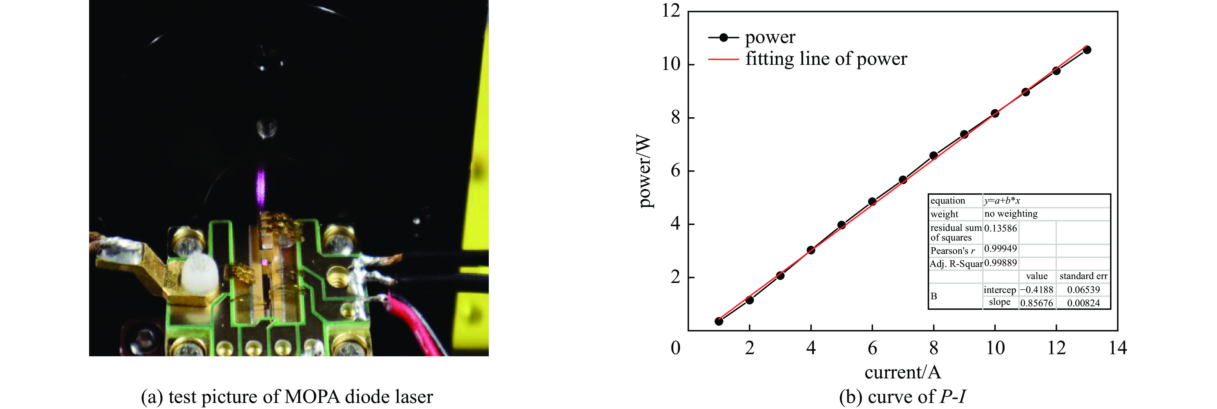
摘要: 结温升高是影响主控振荡放大(MOPA)半导体激光芯片输出功率的重要因素,为解决MOPA芯片的多电极封装和高效散热问题,提出了一种正装和热扩散辅助次热沉相结合的封装结构。建立了该封装结构的3D热模型,对比研究了倒装封装结构、正装无辅助次热沉结构与正装有辅助次热沉结构对MOPA半导体激光器结温的影响。计算结果表明,采用正装有辅助次热沉结构与倒装封装结构散热性能接近,且显著优于正装无辅助次热沉结构,结温降低幅度最高可达40%。另外,采用正装有辅助次热沉封装结构的MOPA半导体激光芯片在连续工作条件下输出功率为10.5 W,谱宽可实现半高全宽小于0.1 nm,中心波长随电流的变化约14 pm/A,实现了10 W级MOPA芯片的封装,验证了该封装结构的有效性。Abstract: The increase in junction temperature is an important factor affecting the output power of master oscillator power amplifier (MOPA) diode laser chip. To achieve the packaging and efficient heat dissipation of the multi-electrode MOPA semiconductor laser chip, a packaging structure that combining P-side up with heat spreader was proposed. An analytical three-dimensional thermal model was employed to study the influence on junction temperature between the P-side down, P-side up without heat spreader and P-side up with heat spreader. According to the three-dimensional thermal model, the conduction-cooled capability between P-side up with heat spreader and P-side down is uniform in this paper. Moreover, the packaging can lead to a maximal 40% decrease on junction temperature. By the way, the P-side up with heat spreader structure was used in MOPA diode laser chip in experiment then 10.5 W output power and the spectrum width (FWHM)<0.1 nm of the MOPA chip were obtained in CW mode.
-
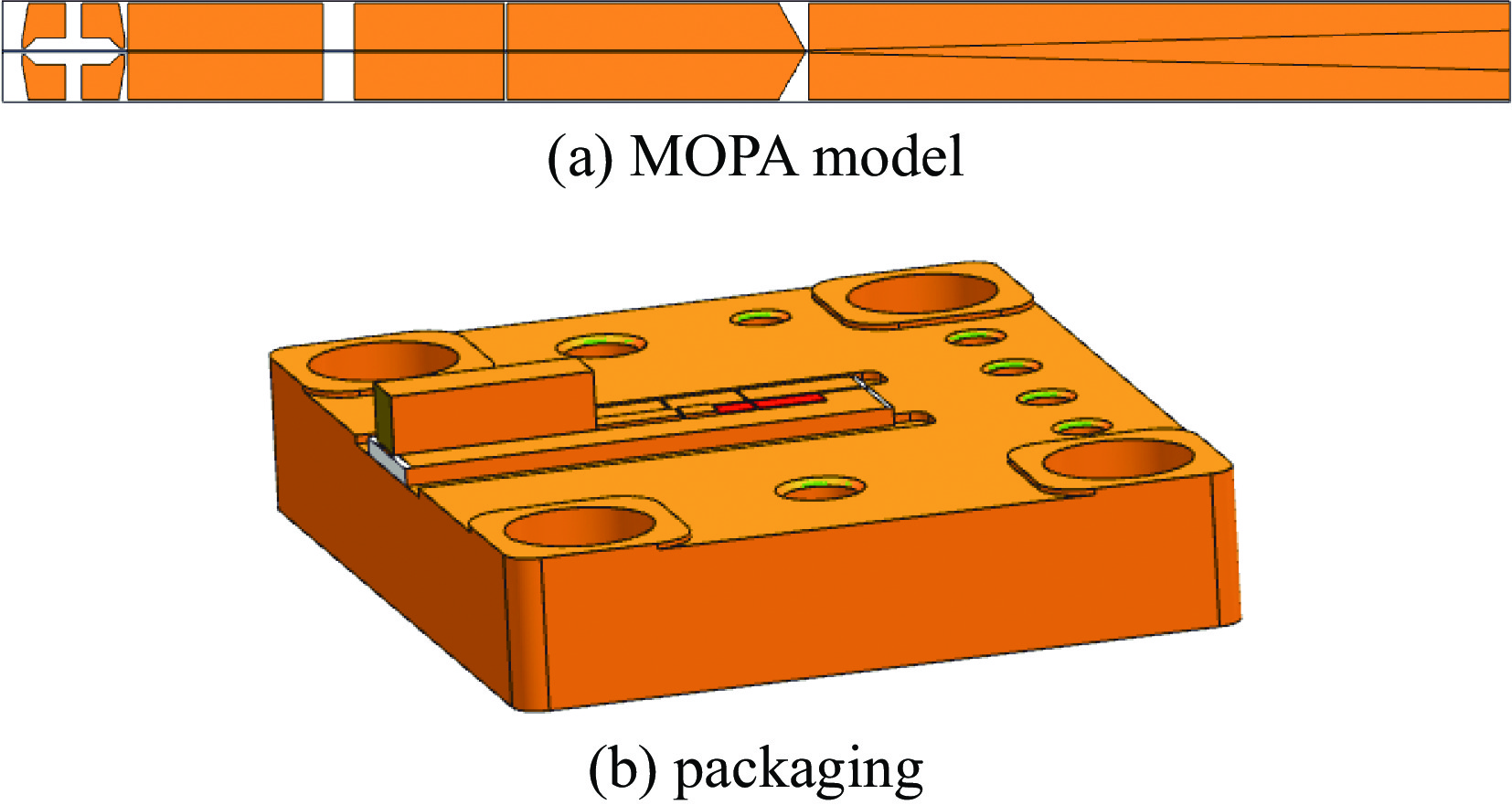
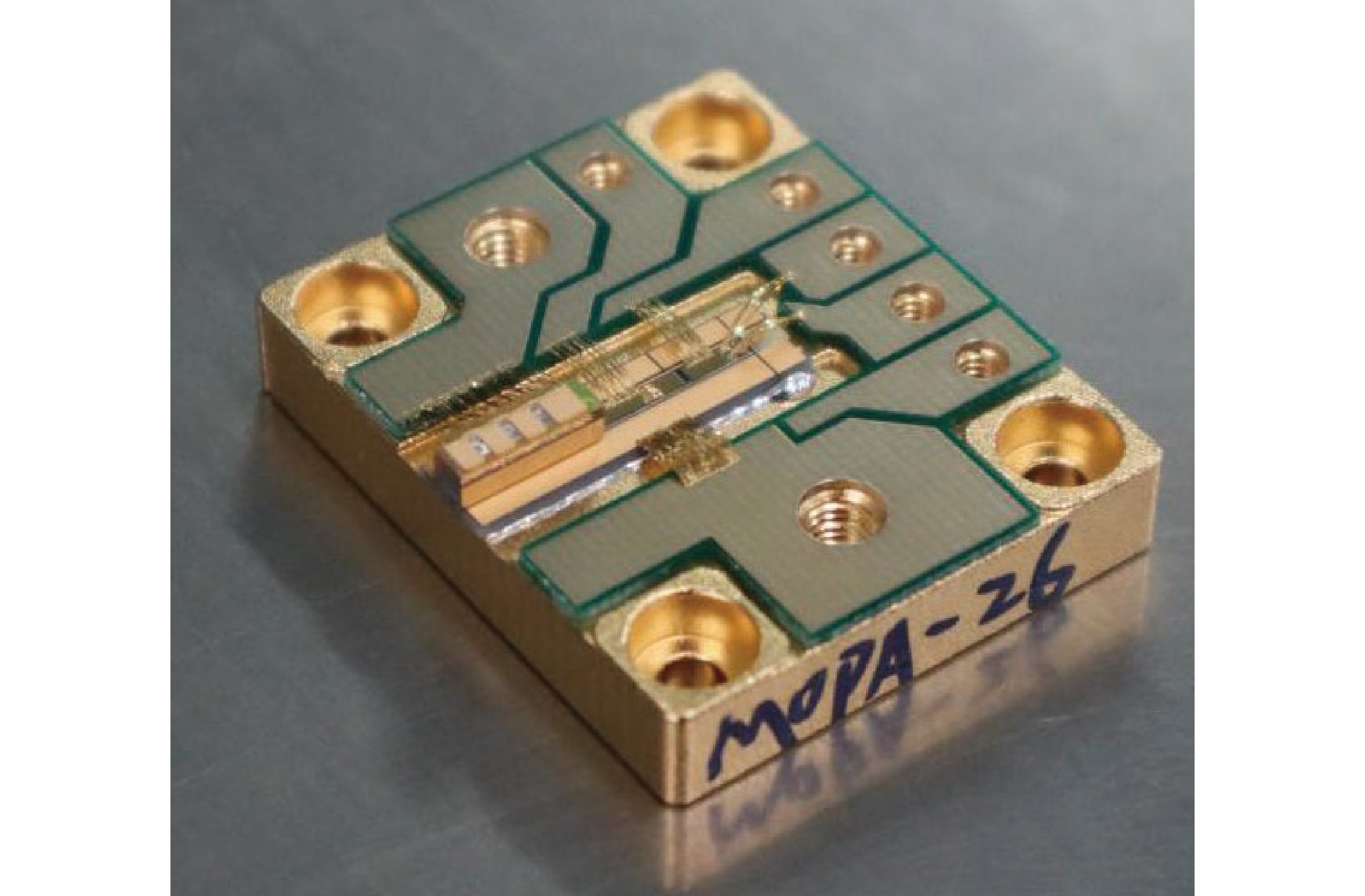
图 2 MOPA芯片结构示意图及封装示意图
Figure 2. Model of MOPA diode laser chip and packaging of the chip
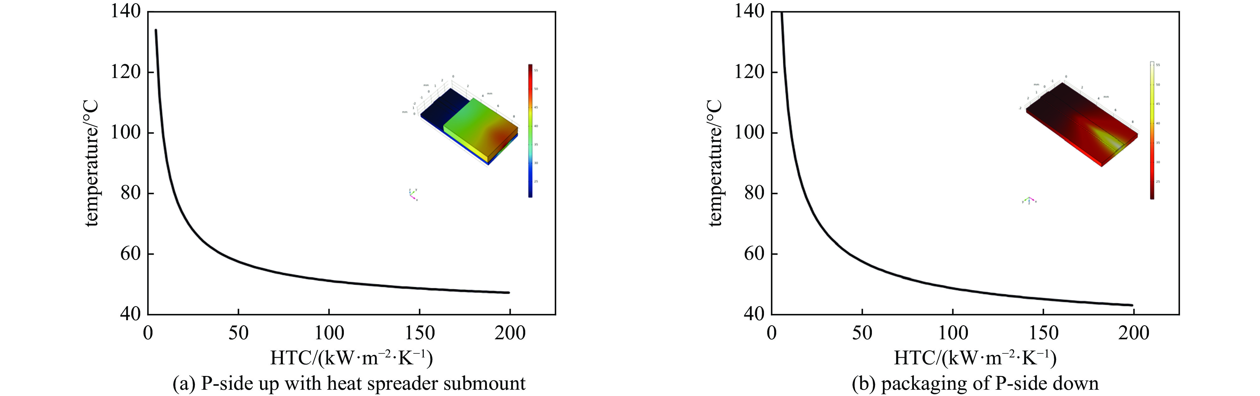
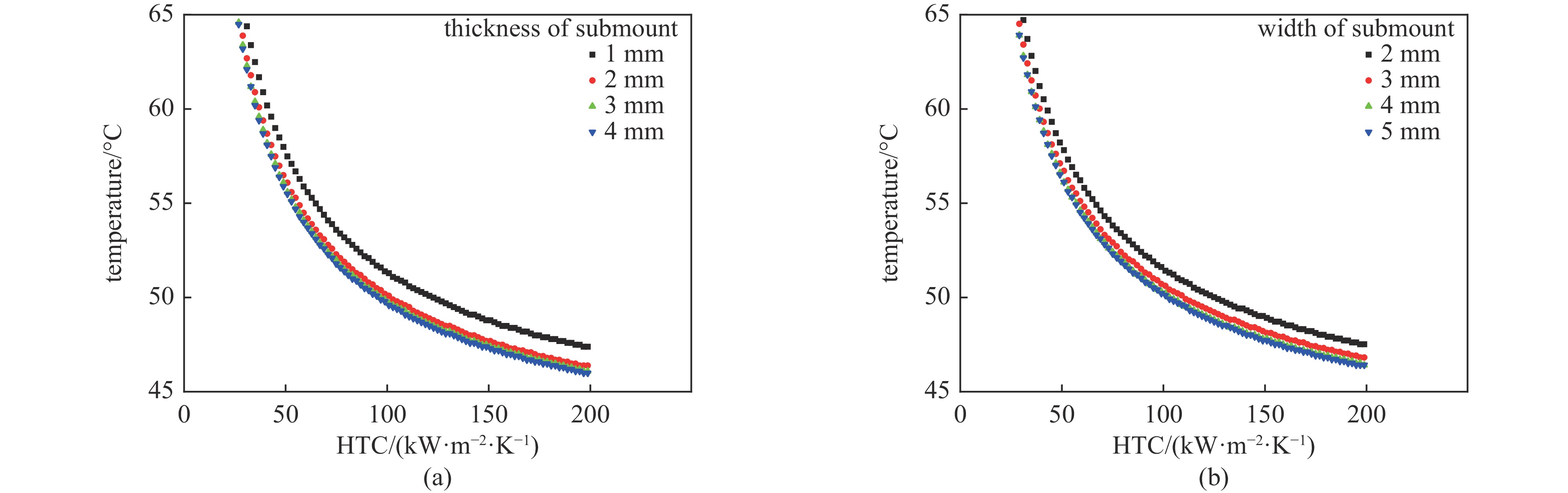
图 4 正装热扩散辅助次热沉与倒装结构对比
Figure 4. Curve of Tj between P-down and P-side up with heat spreader submount
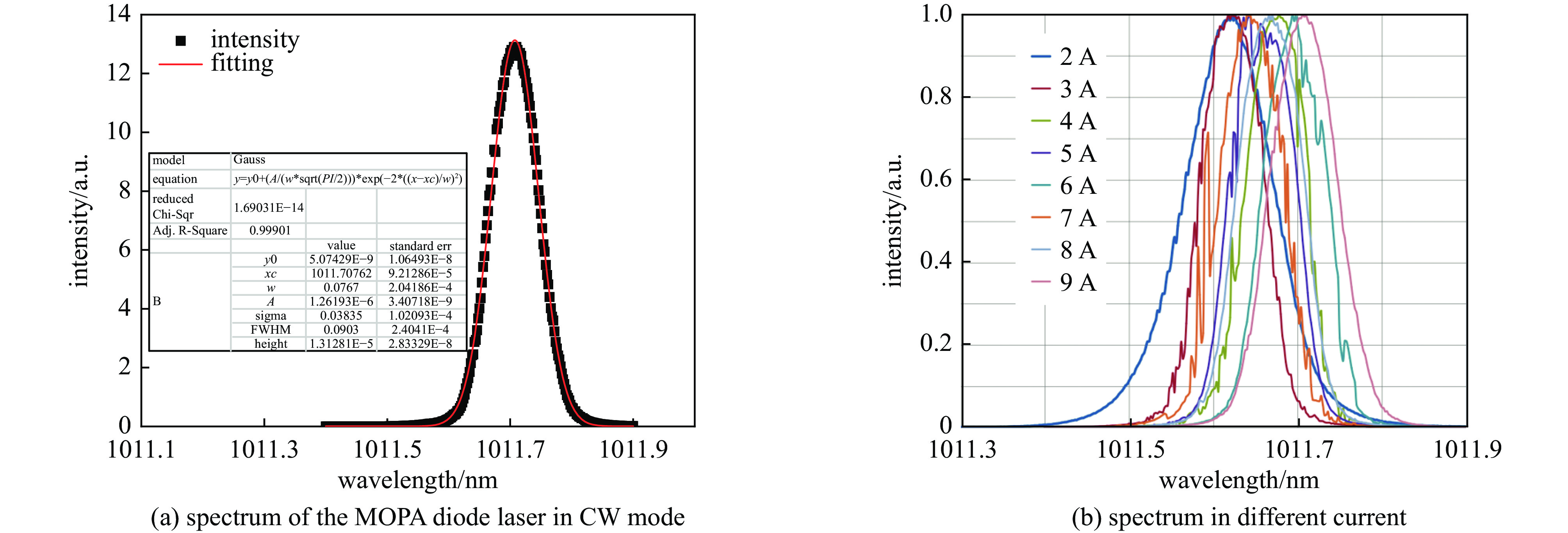
图 9 MOPA芯片连续状态下的输出光谱和不同电流下的光谱变化
Figure 9. Spectrum of the MOPA diode laser in CW mode and the spectrum in different current
表 1 材料参数
Table 1. Material parameters
material thermal conductivity/(W·m−1·K−1) coefficient of thermal expansion/(10−6 K−1) thickness/μm width/mm GaAs 55 6.4 120 1.0 AlN 230 4.5 500 4.5 W90Cu10 180 4.5 1000~3000 2.0~4.5  下载: 导出CSV
-
[1] 孙胜明, 范杰, 徐莉, 等. 锥形半导体激光器研究进展[J]. 中国光学, 2019, 12(1):48-58 doi: 10.3788/co.20191201.0048Sun Shengming, Fan Jie, Xu Li, et al. Progress of tapered semiconductor diode lasers[J]. Chinese Optics, 2019, 12(1): 48-58 doi: 10.3788/co.20191201.0048 [2] 吴涛, 郭栓银. 980 nm高功率锥形激光器巴条的制备及光电特性[J]. 激光与光电子学进展, 2016, 53:041401Wu Tao, Guo Shuanyin. Fabrication and electro-optic properties of 980 nm high-power tapered laser bar[J]. Laser & Optoelectronics Progress, 2016, 53: 041401 [3] Albrodt P, Jamal M T, Hansen A K, et al. Recent progress in brightness scaling by coherent beam combining of tapered amplifiers for efficient high power frequency doubling[C]//Proceedings of SPIE 10900, High-Power Diode Laser Technology XVII. 2019: 109000O. [4] Müller A, Fricke J, Bugge F, et al. DBR tapered diode laser at 1030 nm with nearly diffraction-limited narrowband emission and 12.7 W of optical output power[C]//Proceedings of SPIE 9767, Novel In-Plane Semiconductor Lasers XV. 2016: 97671I. [5] Müller A, Zink C, Fricke J, et al. Efficient, high brightness 1030 nm DBR tapered diode lasers with optimized lateral layout[J]. IEEE Journal of Selected Topics in Quantum Electronics, 2017, 23: 1501107. [6] Müller A, Fricke J, Bugge F, et al. DBR tapered diode laser with 12.7 W output power and nearly diffraction-limited, narrowband emission at 1030 nm[J]. Applied Physics B, 2016, 122: 87. [7] Fiebig C, Blume G, Kaspari C. 12W high-brightness single-frequency DBR tapered diode laser[J]. Electronics Letters, 2008, 44(21): 1253-1255. doi: 10.1049/el:20081371 [8] Zink C, Maaβdorf A, Fricke J, et al. Diffraction limited 1064nm monolithic DBR-master oscillator power amplifier with more than 7W output power[C]//Proceedings of SPIE 10553, Novel In-Plane Semiconductor Lasers XVII. 2018: 105531C. [9] Tawfieq M, Wenzel H, Della Casa P, et al. High-power sampled-grating-based master oscillator power amplifier system with 23.5 nm wavelength tuning around 970 nm[J]. Applied Optics, 2018, 57(29): 8680-8685. doi: 10.1364/AO.57.008680 [10] 张建伟, 宁永强, 张星, 等. 基于载流子注入产热机制的半导体激光器热模型分析[J]. 中国激光, 2012, 39:1002003 doi: 10.3788/CJL201239.1002003Zhang Jianwei, Ning Yongqiang, Zhang Xing, et al. Analysis of the thermal model based on the carrier injection mechanisms within the semiconductor laser[J]. Chinese Journal of Lasers, 2012, 39: 1002003 doi: 10.3788/CJL201239.1002003 [11] Wu Yulong, Dong Zhiyong, Chen Yongqi, et al. Beam shaping for kilowatt fiber-coupled diode lasers by using one-step beam cutting-rotating of prisms[J]. Applied Optics, 2016, 55(34): 9769-9773. doi: 10.1364/AO.55.009769 [12] Wu Dihai, Zah C E, Liu Xingsheng. Thermal design for the package of high-power single-emitter laser diodes[J]. Optics & Laser Technology, 2020, 129: 106266. [13] Mostallino R, Garcia M, Deshayes Y, et al. Thermal investigation on high power dfb broad area lasers at 975nm, with 60% efficiency[C]//Proceedings of SPIE 9733, High-Power Diode Laser Technology and Applications XIV. 2016: 97330S. [14] Fang Junyu, Zhang He, Zou Yonggang, et al. Thermal management of a semiconductor laser array based on a graphite heat sink[J]. Applied Optics, 2019, 58(28): 7708-7715. doi: 10.1364/AO.58.007708 [15] 王娇娇, 石琳琳, 马晓辉, 等. 多单管堆叠半导体激光器热分析及光纤耦合模拟仿真设计[J]. 发光学报, 2021, 42(1):104-110 doi: 10.37188/CJL.20200243Wang Jiaojiao, Shi Linlin, Ma Xiaohui, et al. Thermal analysis and fiber coupling simulation design of multi-single emitters stacked semiconductor laser[J]. Chinese Journal of Luminescence, 2021, 42(1): 104-110 doi: 10.37188/CJL.20200243 [16] Missaggia L J, Huang R K, Chann B, et al. High-power slab-coupled optical waveguide laser array packaging for beam combining[C]//Proceedings of SPIE 6478, Photonics Packaging, Integration, and Interconnects VII. 2007: 647806. -


 点击查看大图
计量
- 文章访问数: 1015
- HTML全文浏览量: 345
- PDF下载量: 118
- 被引次数: 0
