

Parameter optimization design of snubber circuit for high voltage protection switch
-
摘要: 目前的高压保护开关缓冲电路参数设计缺乏相关理论设计方法,同时缓冲电路方案由于设计过程中并未考虑分布电容影响,因此均为等参数设计方案,这种方法均压效果不够理想。为了解决目前参数设计中存在的问题,首先建立了含缓冲电路和杂散电感的MOSFET模型并对其关断过程进行了分析,从而得到了抑制电压尖峰的缓冲电路理论设计方法及表达式。针对串联均压未考虑分布电容的问题,通过构造等电位点,建立了含有分布电容的等效电路并进行分析,根据电荷方程等式得到了缓冲电路非等参数设计方法及表达式,该参数设计方法可以补偿分布电容造成的电压分布不均,并更好地指导高压保护开关的均压方案设计。为了验证参数设计的合理性进行了仿真分析,结果表明,最终得到的整体设计方案可以满足尖峰抑制以及均压的设计要求。Abstract: The ion source and electron gyrotron of the fusion auxiliary heating system are prone to failure and expensive. To protect them, it is necessary to study the high voltage switch scheme. The parameter design methods of high voltage protection switch snubber circuit are lack of relevant theoretical design methods currently, and the snubber circuit schemes are isoparametric design schemes because the influence of distributed capacitance is not taken into account in the design process. The voltage-balancing effect of this method is not ideal. To solve the problems existing in the current parameter design, we have established the MOSFET model with snubber circuit and stray inductor and analyze its turn-off process, thus to obtain the theoretical design method and expression of snubber circuit for suppressing voltage spike. Taking the distributed capacitance into consideration in series voltage-balancing and constructing the isoelectric point, we have established and analyzed the equivalent circuit, and obtained the non-equal parameter design method and expression of snubber circuit according to the charge equation. This parameter design method can compensate the uneven voltage distribution caused by distributed capacitance and guide the voltage-balancing scheme design of high voltage protection switch better. To verify the rationality of the parameter design, we have a carried out, simulation analysis. which shows that the overall design scheme can meet the design requirements of peak suppression and voltage-balancing.
-
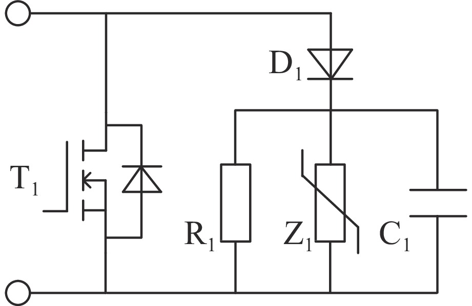
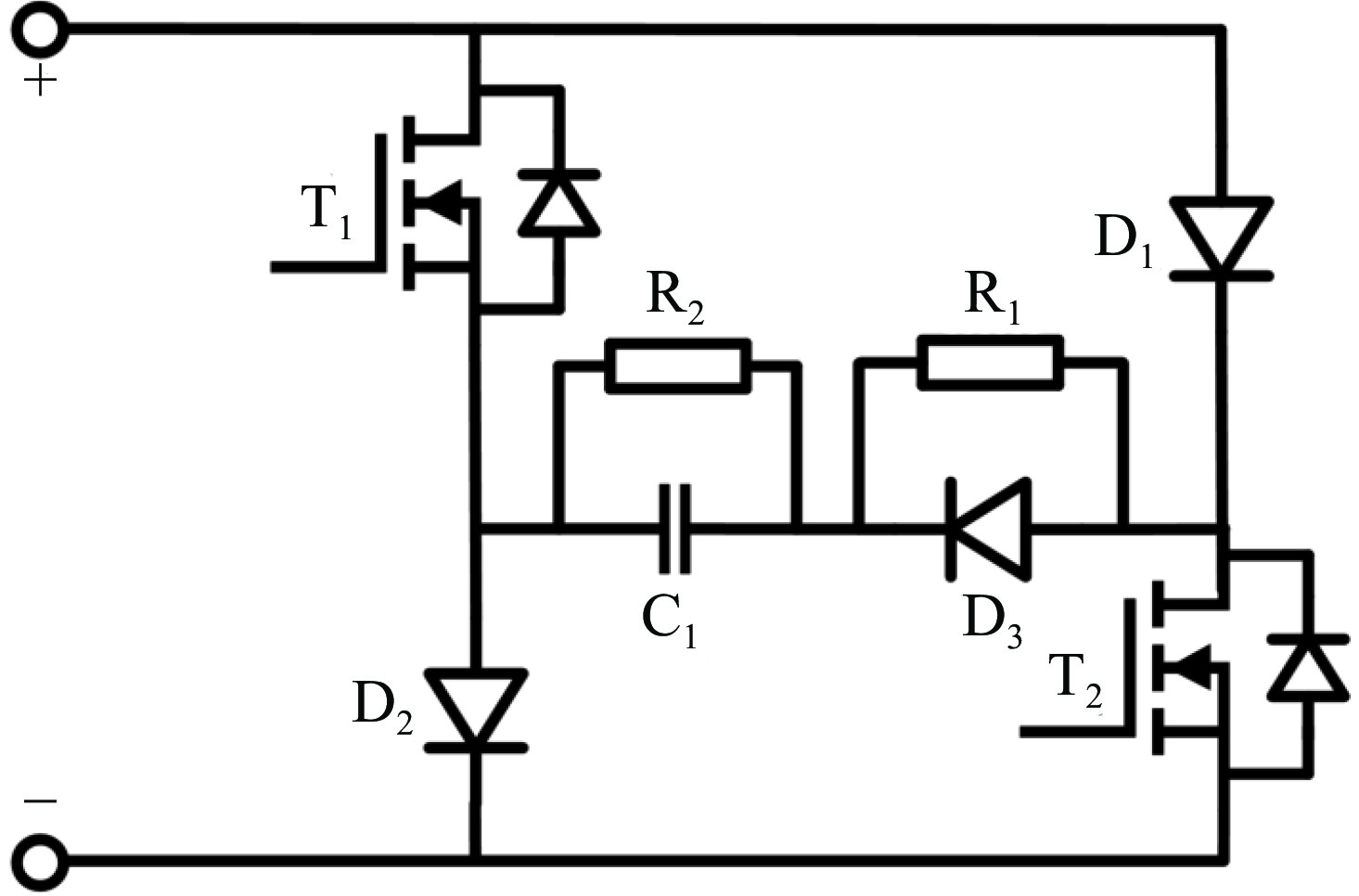
图 1 电压钳位型均压电路原理图
Figure 1. Schematic diagram of voltage clamp voltage-balancing circuit
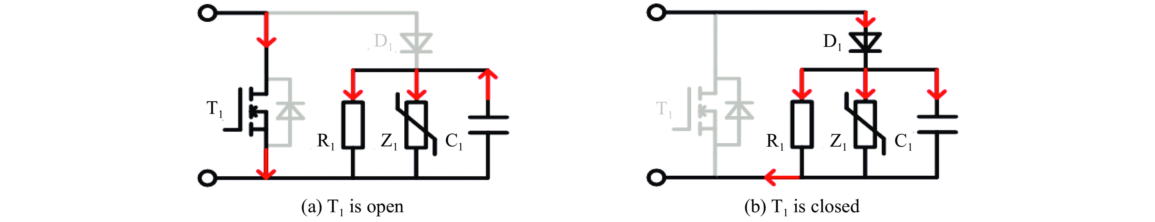
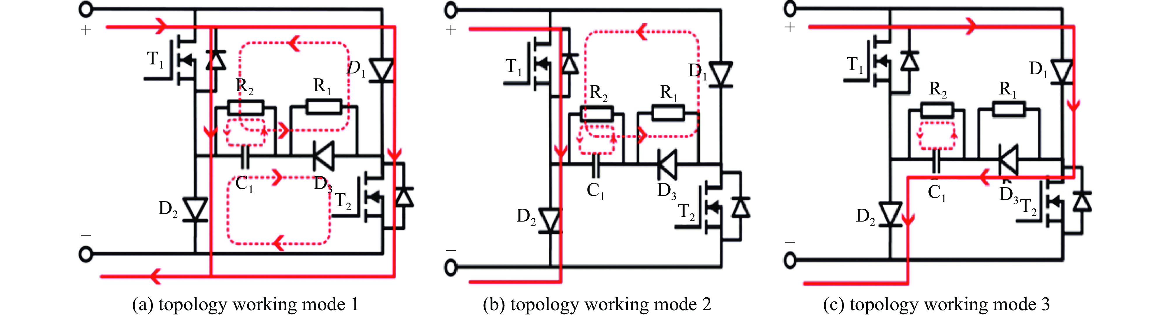
图 2 电压钳位型均压电路工作原理图
Figure 2. Working principle diagram of voltage clamp voltage-balancing circuit
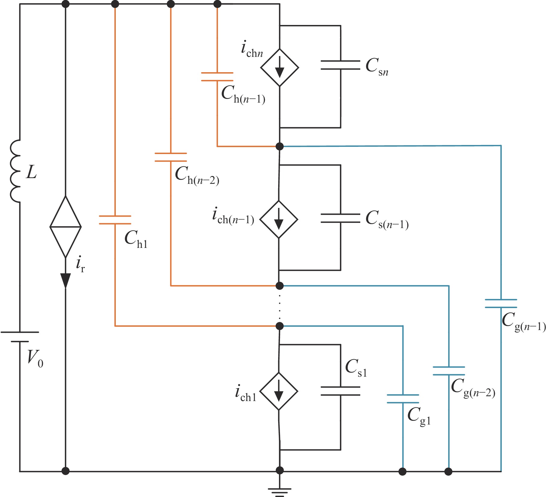
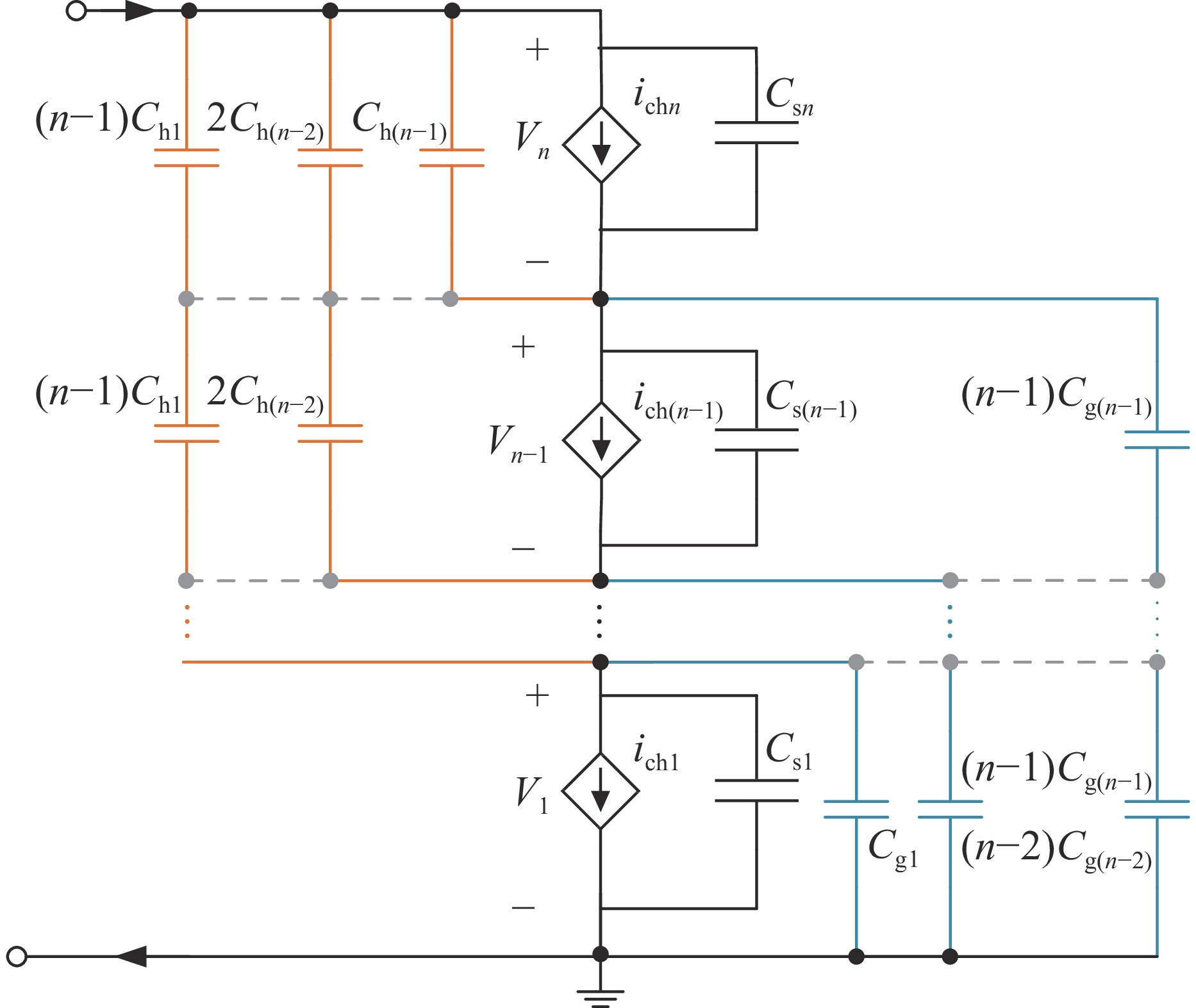
图 8 考虑分布电容和缓冲电路的串联MOSFET等效电路
Figure 8. Equivalent circuit of series MOSFET considering distributed capacitor and snubber circuit
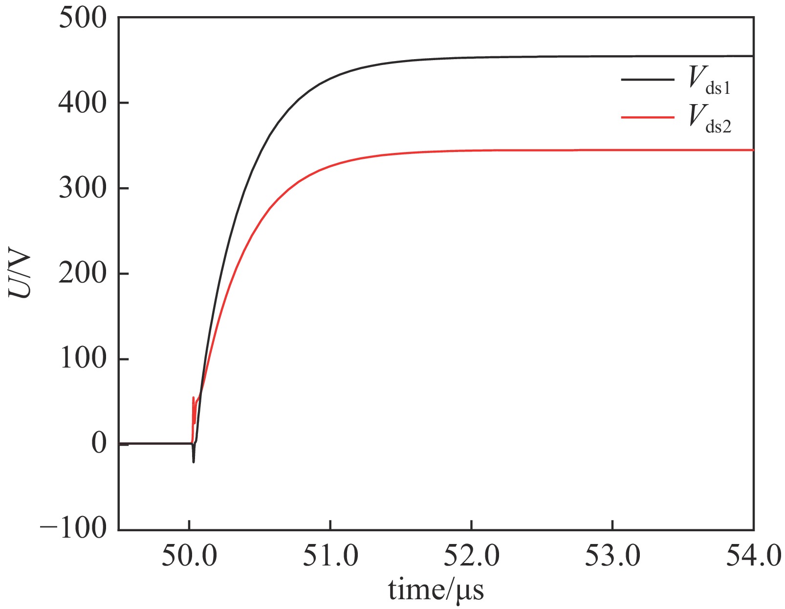
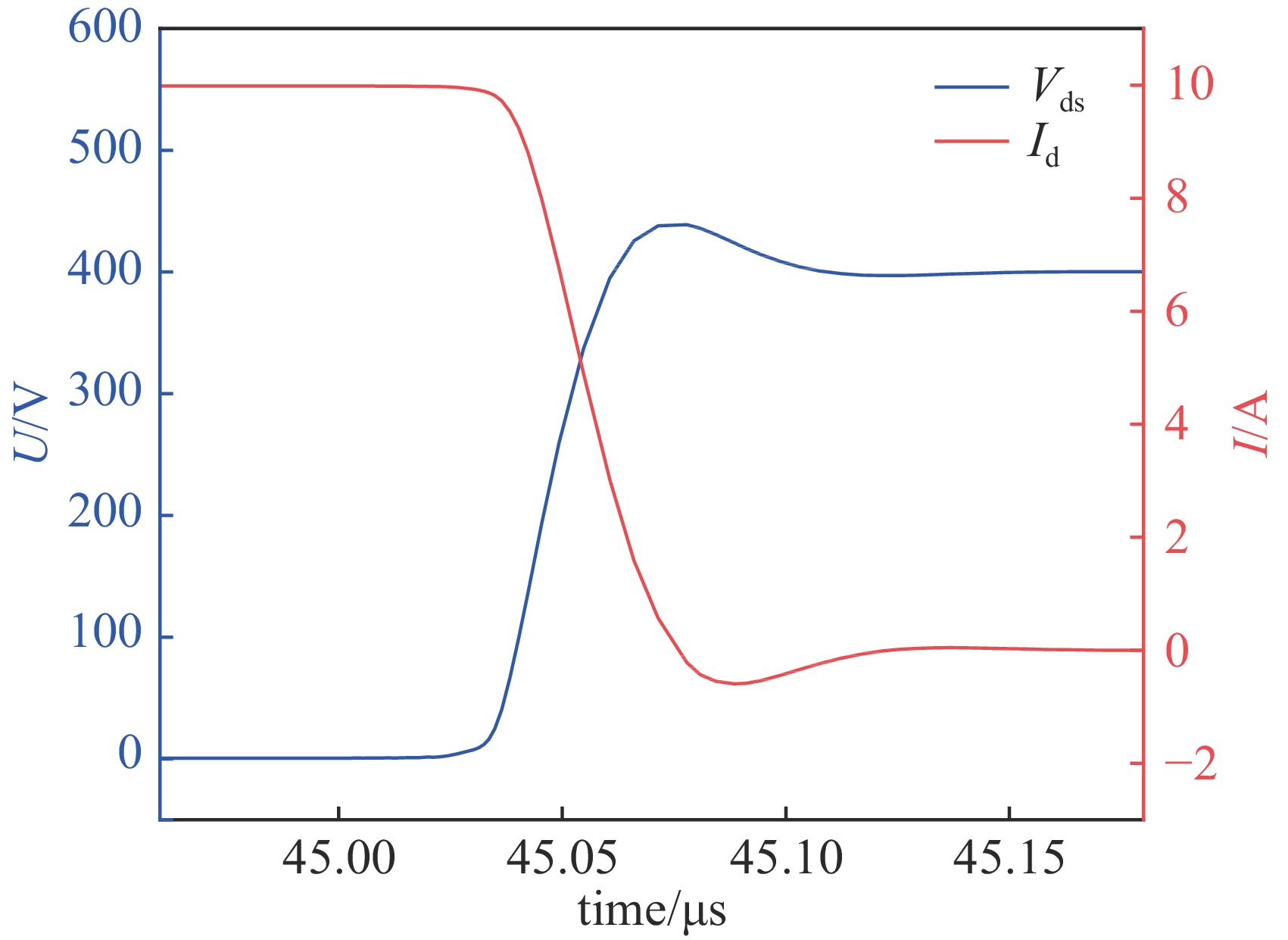
图 15 等参数缓冲电路的两管电压波形图
Figure 15. Two-tube voltage waveform of isoparametric snubber circuit
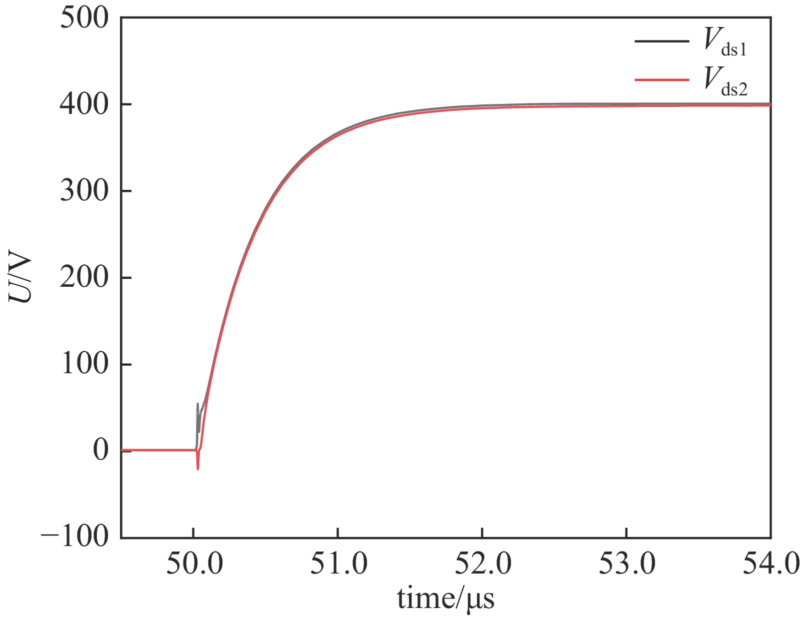
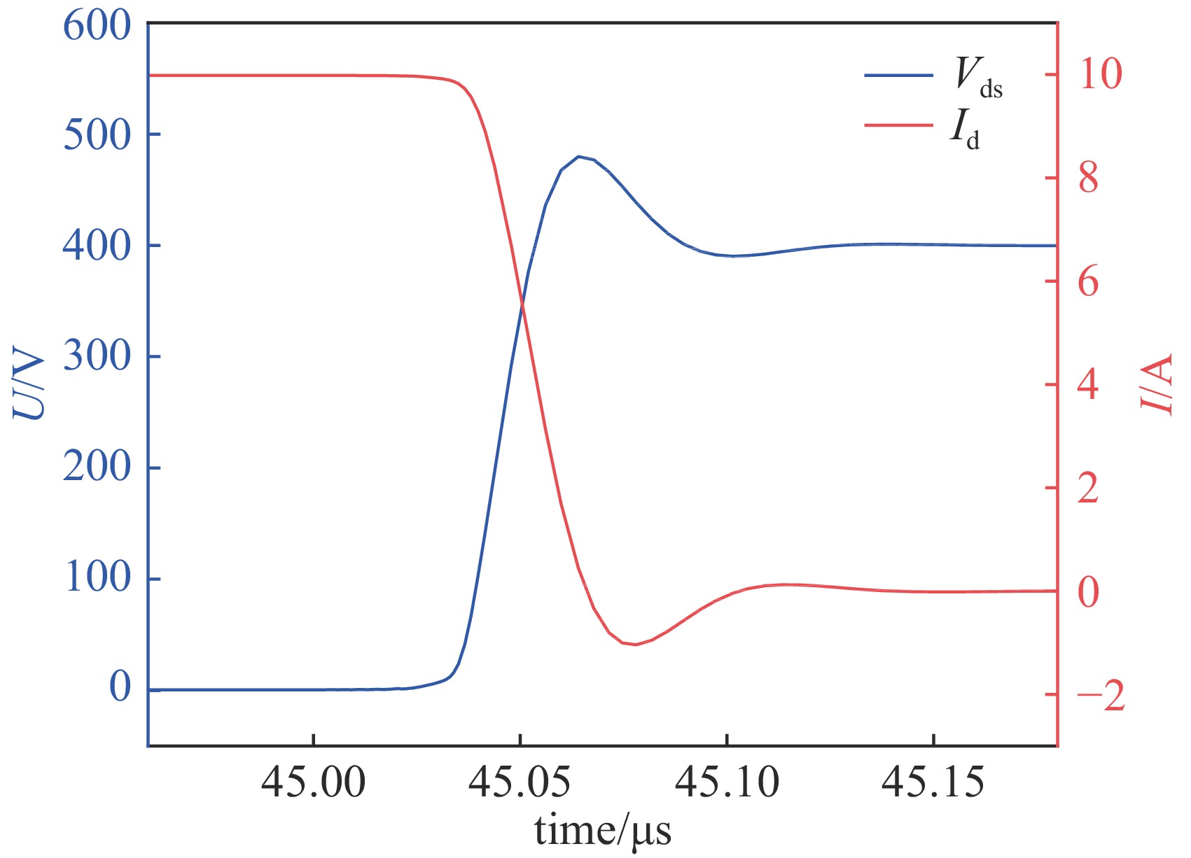
图 16 非等参数缓冲电路的两管电压波形图
Figure 16. Two-tube voltage waveform of non-isoparametric snubber circuit
表 1 拓扑工作模式
Table 1. Topology working mode
pattern T1 T2 module voltage single tube current function 1 on on 0 i1/2 over-current balancing 2 on off 0 i1 conduction discharge 3 off off V1 0 current shutoff 4 off on 0 i1 conduction discharge  下载: 导出CSV
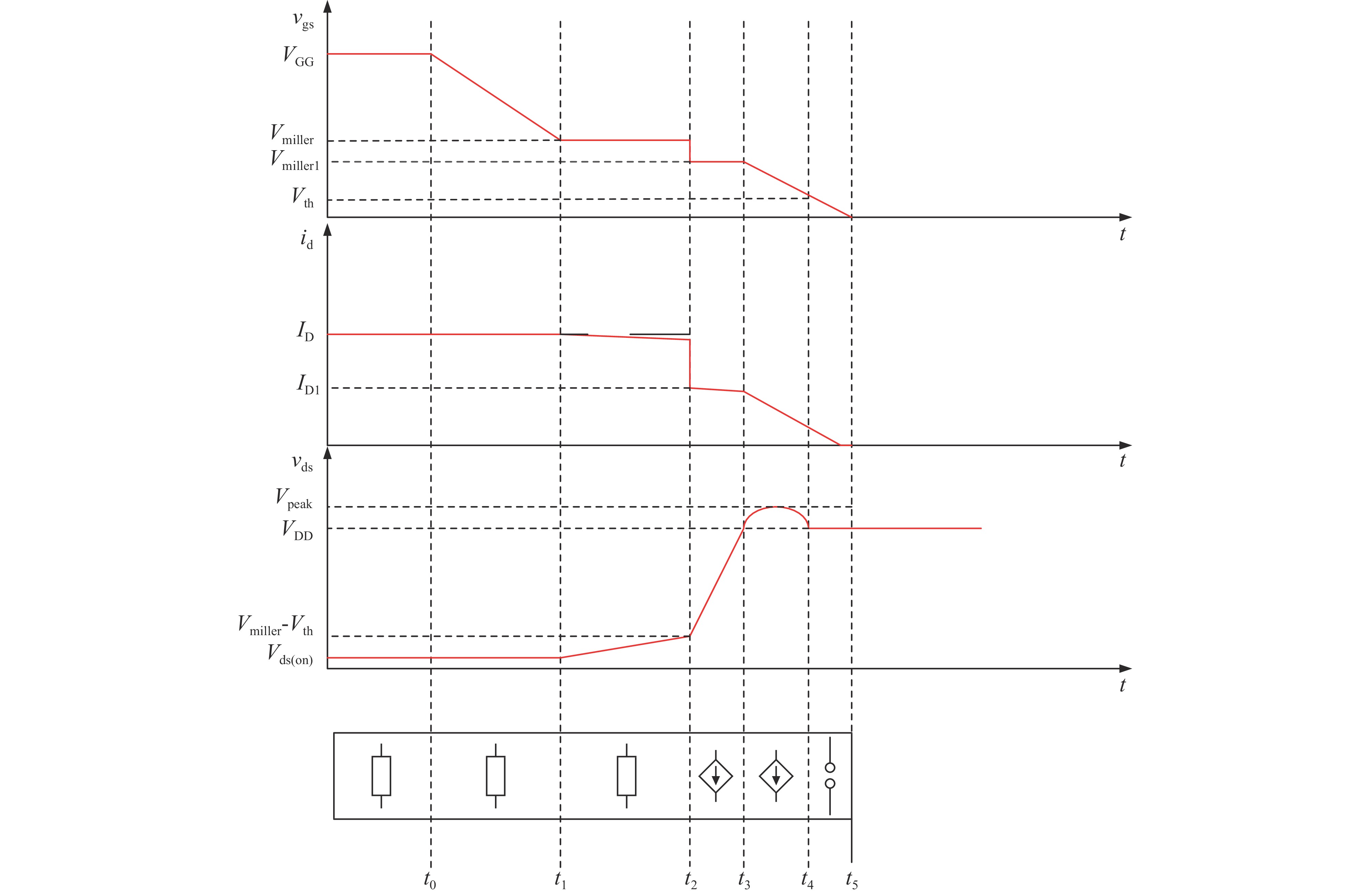
表 2 MOSFET工作模式
Table 2. Working modes of MOSFET
operation mode Cgs Cgd Cds channel condition Vgs>Vth and Vds≤Vgs−Vth Ohmic Cgs Cgd2 Cds2 constant resistance Rds(on) Vgs<Vth cut off Cgs Cgd1 Cds1 open circuit
下载: 导出CSV
-
[1] 章雪亮. 聚变装置辅助加热系统逆变型直流高压电源技术研究[D]. 武汉: 华中科技大学, 2016Zhang Xueliang. Research on the technology of inverter type DC high voltage power supply for auxiliary heating system of fusion device[D]. Wuhan: Huazhong University of Science & Technology, 2016 [2] Watanabe K, Kashiwagi M, Kawashima S, et al. Development of a dc 1 MV power supply technology for NB injectors[J]. Nuclear Fusion, 2006, 46(6): S332-S339. doi: 10.1088/0029-5515/46/6/S15 [3] 余振雄. J-TEXT装置ECRH控制系统研究[D]. 武汉: 华中科技大学, 2017Yu Zhenxiong. Research of electron cyclotron resonance heating control system on J-TEXT[D]. Wuhan: Huazhong University of Science and Technology, 2017 [4] Zhang Ming, Wang Dongyu, Ma Shaoxiang, et al. A novel series switch module in high-voltage applications[J]. Fusion Engineering and Design, 2019, 146: 2618-2623. doi: 10.1016/j.fusengdes.2019.04.057 [5] Abbate C, Busatto G, Iannuzzo F. High-voltage, high-performance switch using series-connected IGBTs[J]. IEEE Transactions on Power Electronics, 2010, 25(9): 2450-2459. doi: 10.1109/TPEL.2010.2049272 [6] Podlesak T F, Carter J L, McMurray J A. Demonstration of compact solid-state opening and closing switch utilizing GTOs in series[J]. IEEE Transactions on Electron Devices, 1991, 38(4): 706-711. doi: 10.1109/16.75193 [7] Consoli A, Musumeci S, Oriti G, et al. Active voltage balancement of series connected IGBTs[C]//Proceedings of the Conference Record of the 1995 IEEE Industry Applications Conference Thirtieth IAS Annual Meeting. 1995: 2754-2758. [8] Renz G, Holzschuh F, Zeyfang E. PFNs switched with stacked SCRs at 20 kV, 500 J, and 100 Hz REP-rate[C]//Proceedings of the 11th IEEE International Pulsed Power Conference. 1997: 390-395. [9] Welleman A, Fleischmann W, Kaesler W. Solid state on-off pulse switches using IGCT technology[C]//Proceedings of the IEEE 34th International Conference on Plasma Science. 2007: 1025-1028. [10] Dongye Zhonghao, Qi Lei, Cui Xiang, et al. A new approach to model reverse recovery process of a thyristor for HVdc circuit breaker testing[J]. IEEE Transactions on Power Electronics, 2021, 36(2): 1591-1601. doi: 10.1109/TPEL.2020.3007660 [11] Luo Yifei, Xiao Fei, Liu Binli, et al. A physics-based transient electrothermal model of high-voltage press-pack IGBTs under HVdc interruption[J]. IEEE Transactions on Power Electronics, 2020, 35(6): 5660-5669. doi: 10.1109/TPEL.2019.2948936 [12] Xiao Huangqing, Xu Zheng, Xiao Liang, et al. Components sharing based integrated HVDC circuit breaker for meshed HVDC grids[J]. IEEE Transactions on Power Delivery, 2020, 35(4): 1856-1866. doi: 10.1109/TPWRD.2019.2955726 [13] Wang Dongyu, Zhang Ming, Ma Shaoxiang, et al. A high-voltage solid-state switch based on submodule topology of SiC MOSFETs for J-TEXT tokamak[J]. IEEE Transactions on Plasma Science, 2020, 48(6): 1676-1680. doi: 10.1109/TPS.2019.2959623 [14] Ma Shaoxiang, Shang Wentong, Wang Dongyu, et al. A reliable voltage clamping submodule based on SiC MOSFET for solid state switch[J]. Review of Scientific Instruments, 2021, 92: 024713. doi: 10.1063/5.0027135 [15] Lu Ting, Zhao Zhengming, Ji Shiqi, et al. Active clamping circuit with status feedback for series-connected HV-IGBTs[J]. IEEE Transactions on Industry Applications, 2014, 50(5): 3579-3590. doi: 10.1109/TIA.2014.2308356 [16] Ji Shiqi, Lu Ting, Zhao Zhengming, et al. Series-connected HV-IGBTs using active voltage balancing control with status feedback circuit[J]. IEEE Transactions on Power Electronics, 2015, 30(8): 4165-4174. doi: 10.1109/TPEL.2014.2360189 [17] Zarghani M, Mohsenzade S, Kaboli S. A fast and series-stacked IGBT switch with balanced voltage sharing for pulsed power applications[J]. IEEE Transactions on Plasma Science, 2016, 44(10): 2013-2021. doi: 10.1109/TPS.2016.2574126 -


 点击查看大图
计量
- 文章访问数: 867
- HTML全文浏览量: 269
- PDF下载量: 130
- 被引次数: 0
