

Performance research and parameter optimization of 15 nm Bulk nFinFET device
-
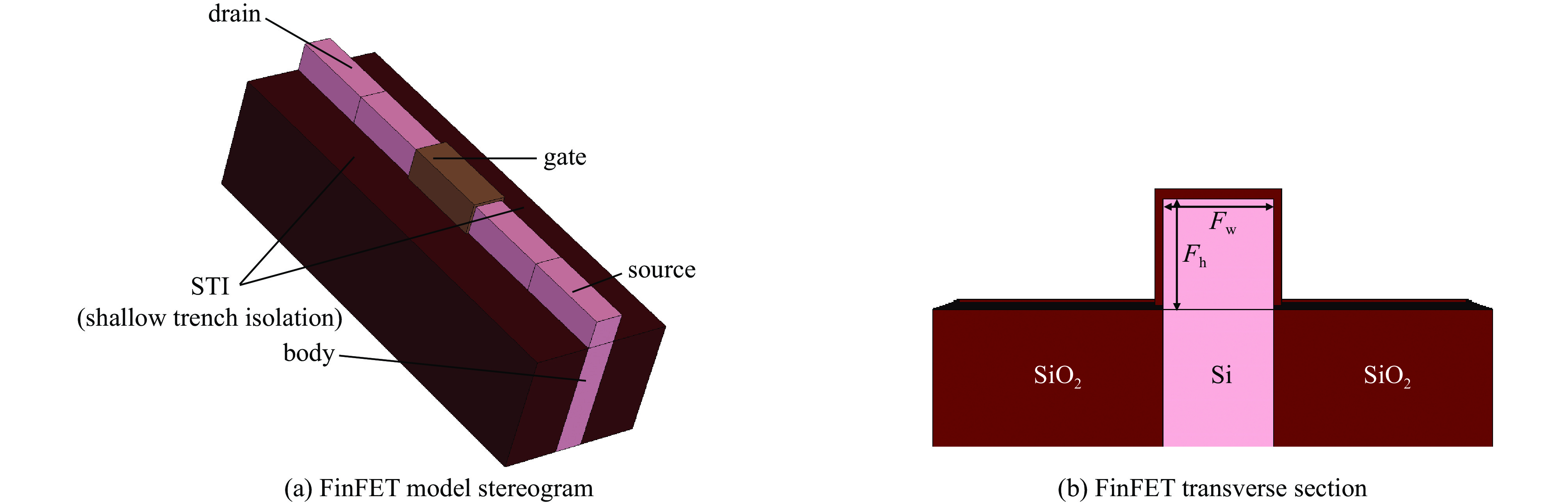
摘要: 为研究Bulk FinFET工作时基本结构参数、器件温度和栅极材料对其性能的影响,建立了一个15 nm n型Bulk FinFET器件模型,仿真分析了不同栅长、鳍宽、鳍高、沟道掺杂浓度、器件工作温度、栅极材料对器件性能的影响,发现增长栅长、降低鳍宽和增加鳍高有助于抑制短沟道效应;1×1017 cm−3以下的低沟道掺杂浓度对器件特性影响不大,但高掺杂会使器件失效;器件工作温度的升高会导致器件性能的下降;采用高K介质材料作为栅极器件性能优于传统材料SiO2。
-
关键词:
- Bulk FinFET /
- 短沟道效应 /
- 器件性能 /
- 参数优化 /
- 栅极材料
Abstract: Due to the growing severity of the short-channel effect in semiconductor devices, a new type of device, the FinField-Effect Transistor (FinFET), has been proposed, developed and applied. This paper aims to establish a 15 nm n-type Bulk FinFET device model to investigate the impact of basic structural parameters, device temperature, and gate material on the performance of Bulk FinFETs. Simulations are conducted to analyze the effect of different gate lengths, fin widths, fin heights, channel doping concentration, device operating temperature, and gate materials on the performance of FinFETs. The results show that increasing the gate length, decreasing the fin width, and increasing the fin height can effectively suppress the short-channel effect. Moreover, the channel doping concentration below 1×1017 cm−3 has little effect on the device characteristics, while high doping concentration causes device failure. Additionally, increasing the operating temperature leads to device performance degradation. Finally, using high K dielectric material as the gate material is found to enhance device performance compared to using conventional SiO2 material.-
Key words:
- Bulk FinFET /
- short channel effect /
- device performance /
- parameter optimization /
- gate material
-
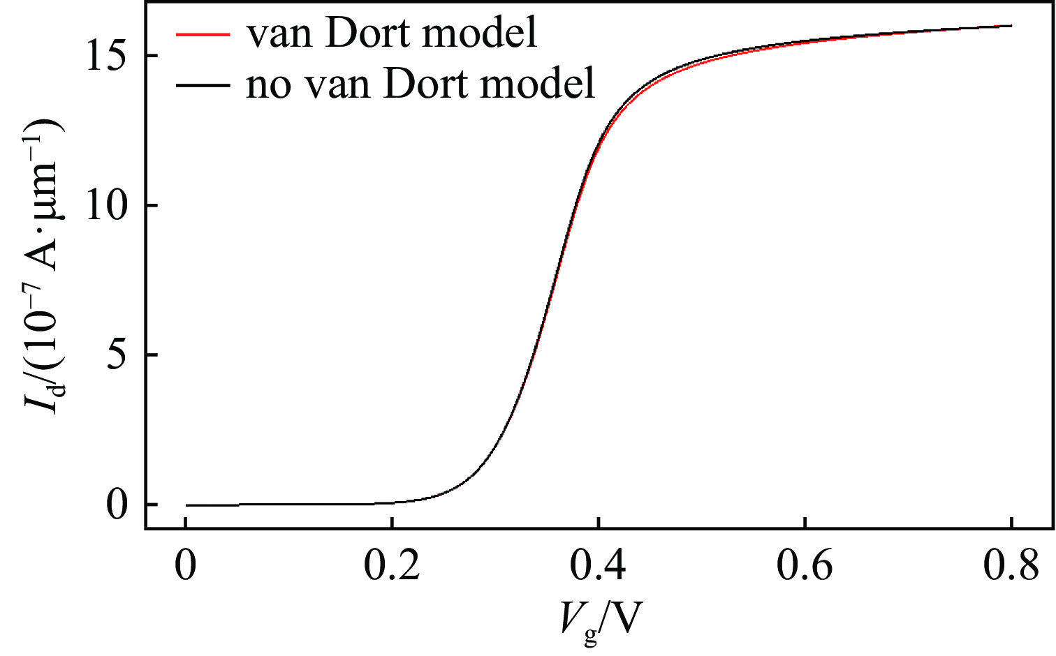
图 2 添加量子修正项与不添加量子修正项的Id-Vg曲线对比图
Figure 2. Comparison of Id-Vg curves with and without quantum correction items
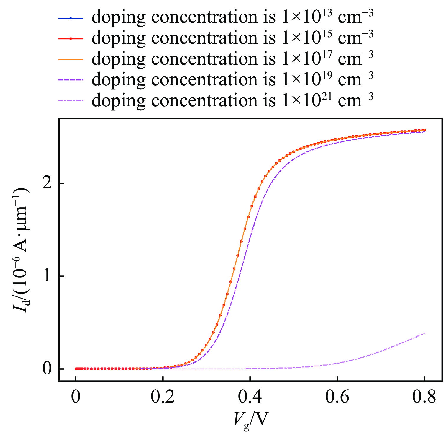
图 10 不同沟道掺杂浓度下的Id-Vg曲线
Figure 10. Id-Vg curves with different channel doping concentrations
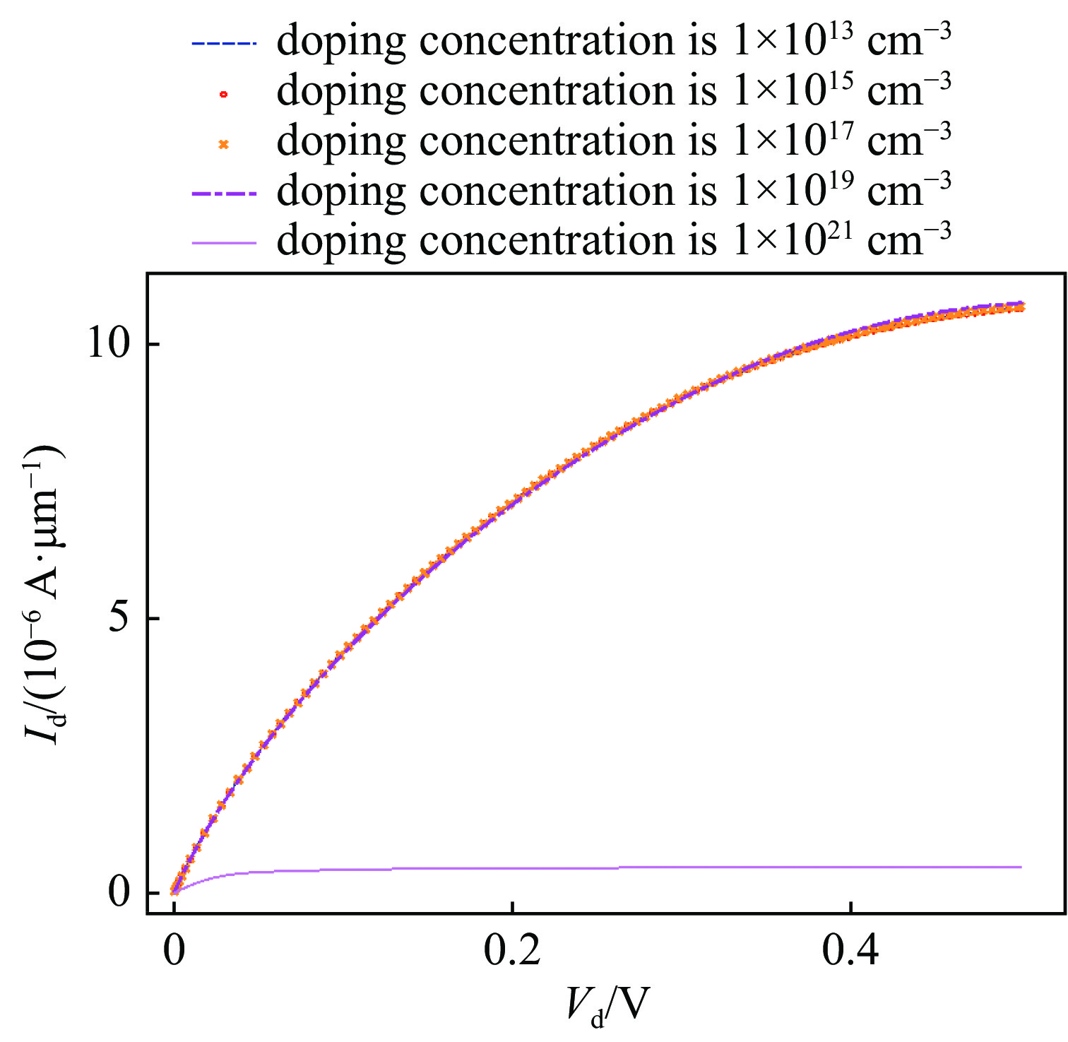
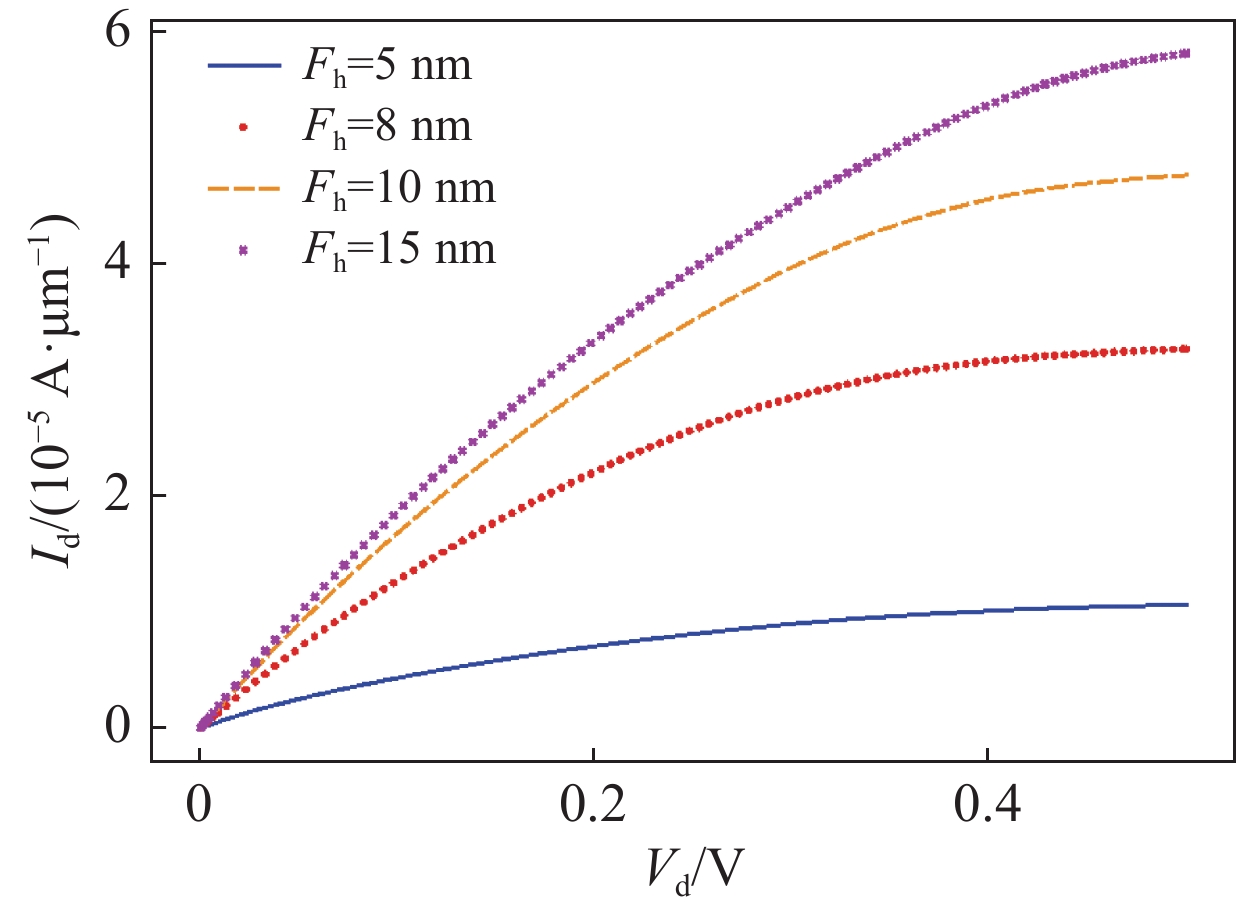
图 11 不同沟道掺杂浓度下的Id-Vd曲线
Figure 11. Id-Vd curves with different channel doping concentrations
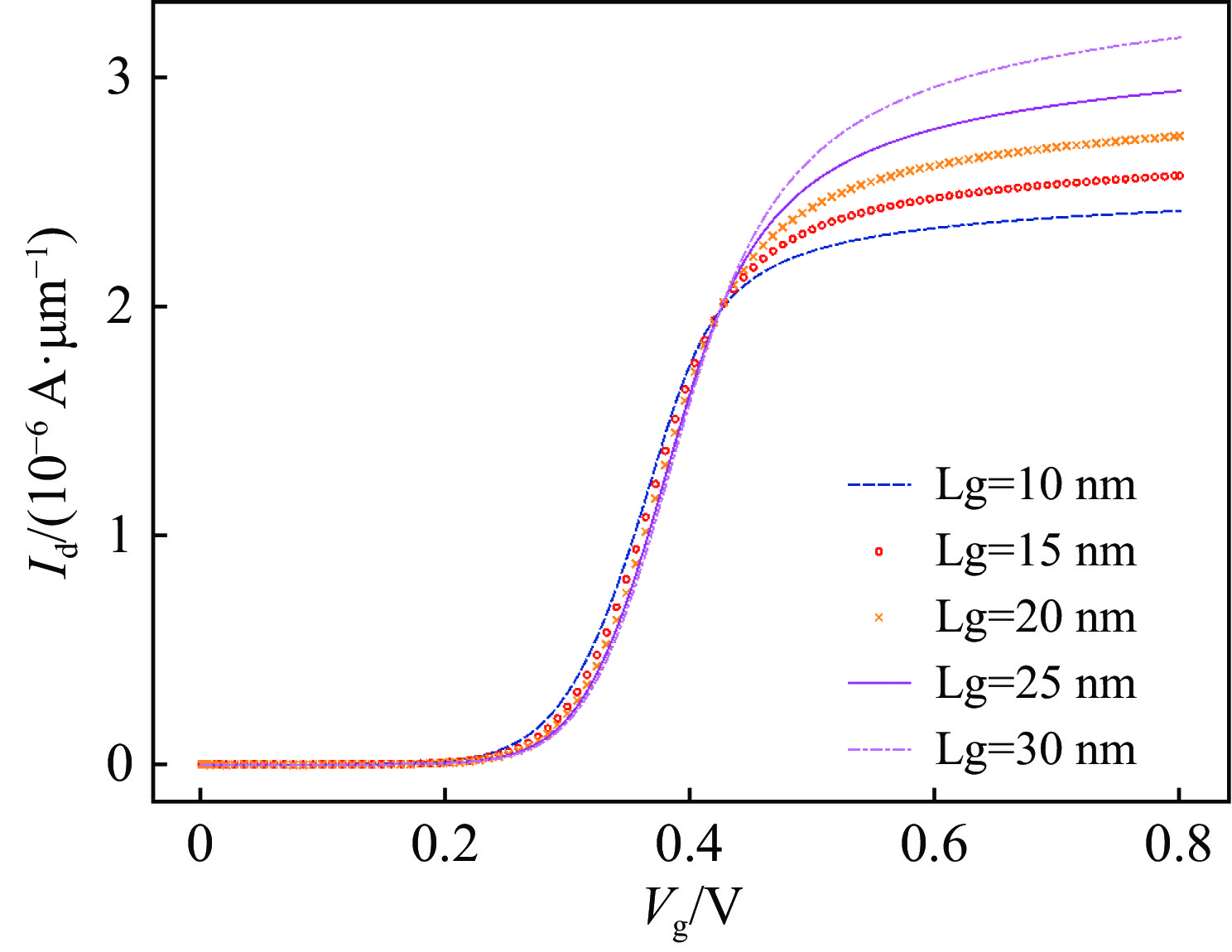
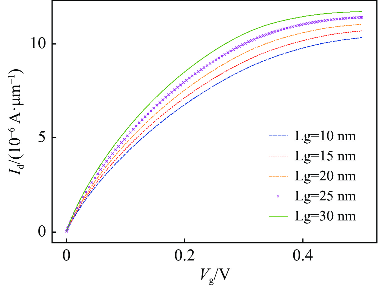
表 1 不同栅长下VT、SS、DIBL
Table 1. VT, SS and DIBL under different gate lengths
gate length/nm VT/V SS/mV DIBL/(mV·V−1) 10 0.3058 72.0845 20.53 15 0.3041 67.6268 18.55 20 0.3082 65.1960 12.57 25 0.3117 64.0744 0.92 30 0.3149 63.4691 0.80  下载: 导出CSV
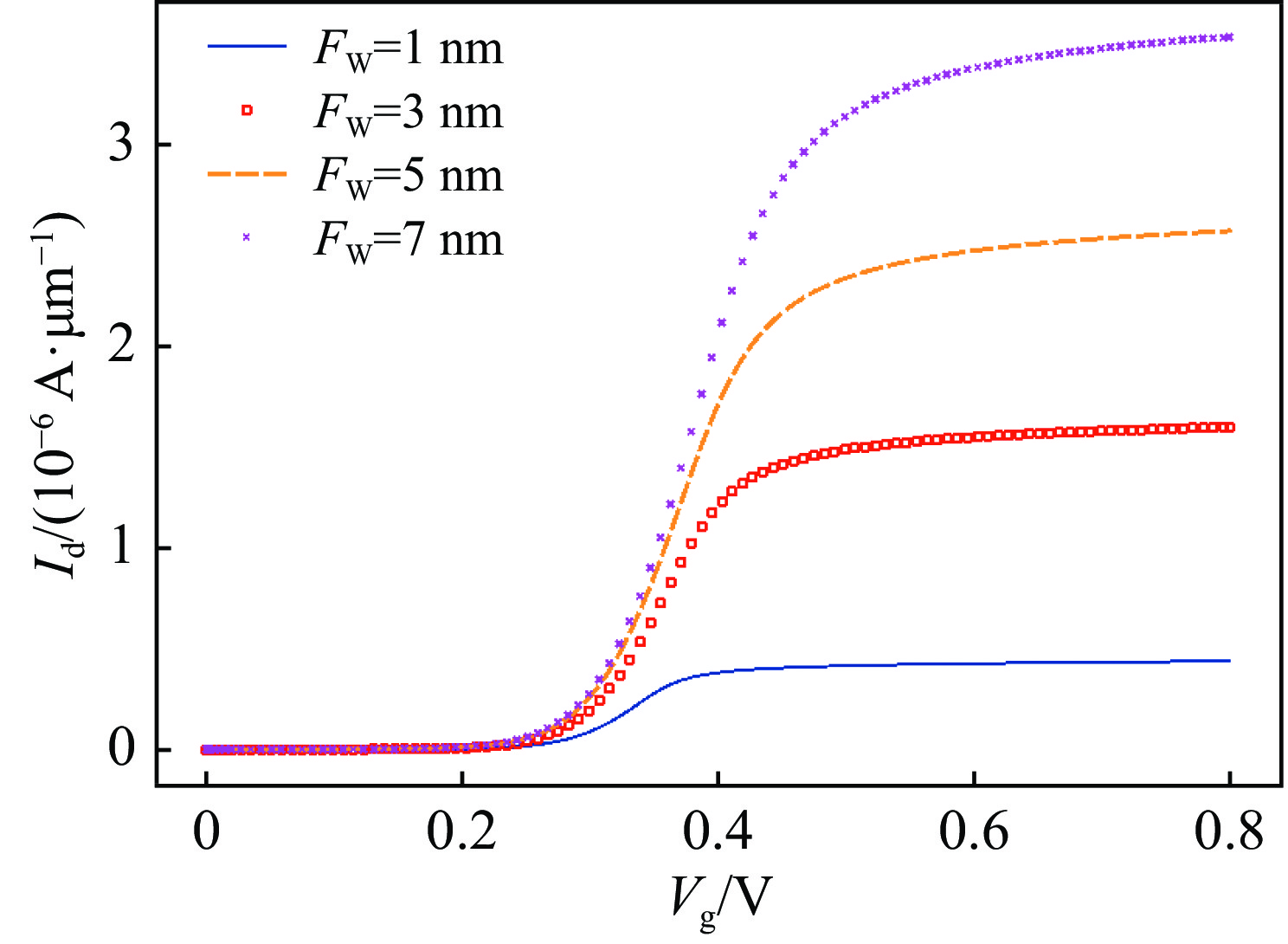
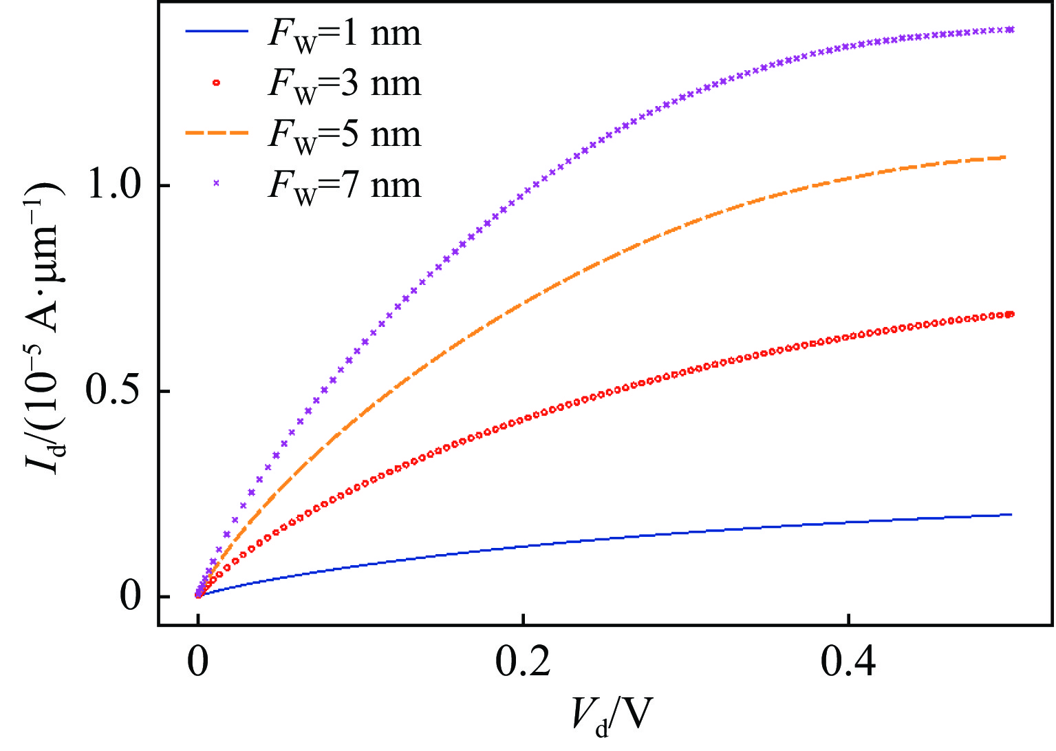
表 2 不同鳍宽下VT、SS、DIBL
Table 2. VT, SS and DIBL under different fin widths
fin width/nm VT/V SS/mV DIBL/(mV·V−1) 1 0.3041 67.6269 5.42 3 0.3178 75.1745 10.84 5 0.3241 82.8697 18.53 7 0.3306 89.7392 25.62
下载: 导出CSV
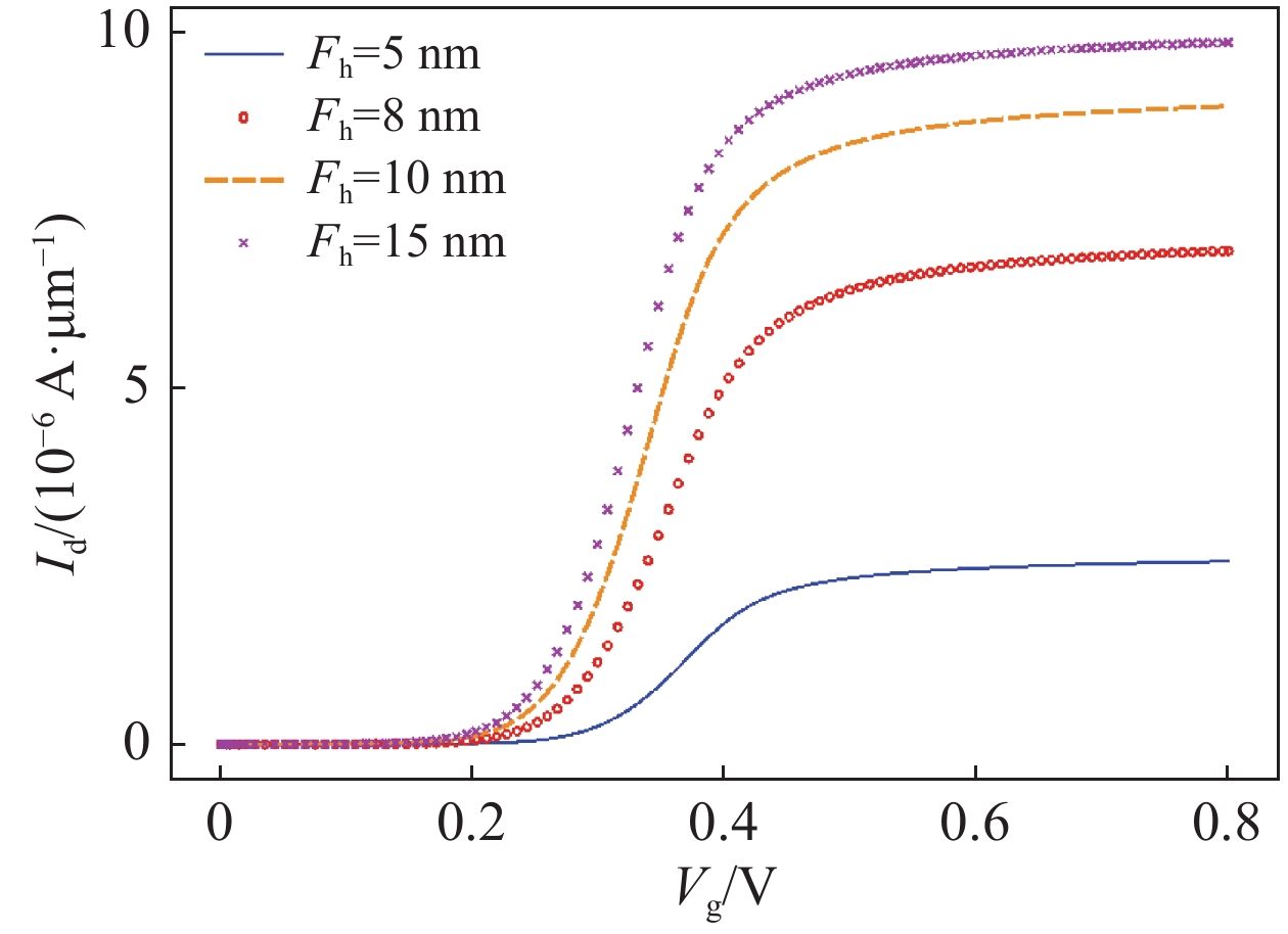
表 3 不同鳍高下VT、SS、DIBL
Table 3. VT, SS and DIBL under different fin heights
fin height/nm VT/V SS/mV DIBL/(mV·V−1) 5 0.3045 70.5220 63.03 8 0.3051 69.0909 61.46 10 0.3041 67.6269 59.80 15 0.2983 65.4408 57.38 18 0.2937 67.1448 54.73
下载: 导出CSV
表 4 不同沟道掺杂浓度下VT、SS、DIBL
Table 4. VT, SS and DIBL under different channel doping concentrations
channel doping
concentration/cm−3VT/V SS/mV DIBL/(mV·V−1) 1×10¹³ 0.3042 67.5652 21.19 1×10¹⁵ 0.3041 67.5704 21.33 1×10¹⁷ 0.3041 67.6269 19.70 1×10¹⁹ 0.3166 67.6392 44.29 1×10²¹ 0.6179 76.4825 97.29
下载: 导出CSV
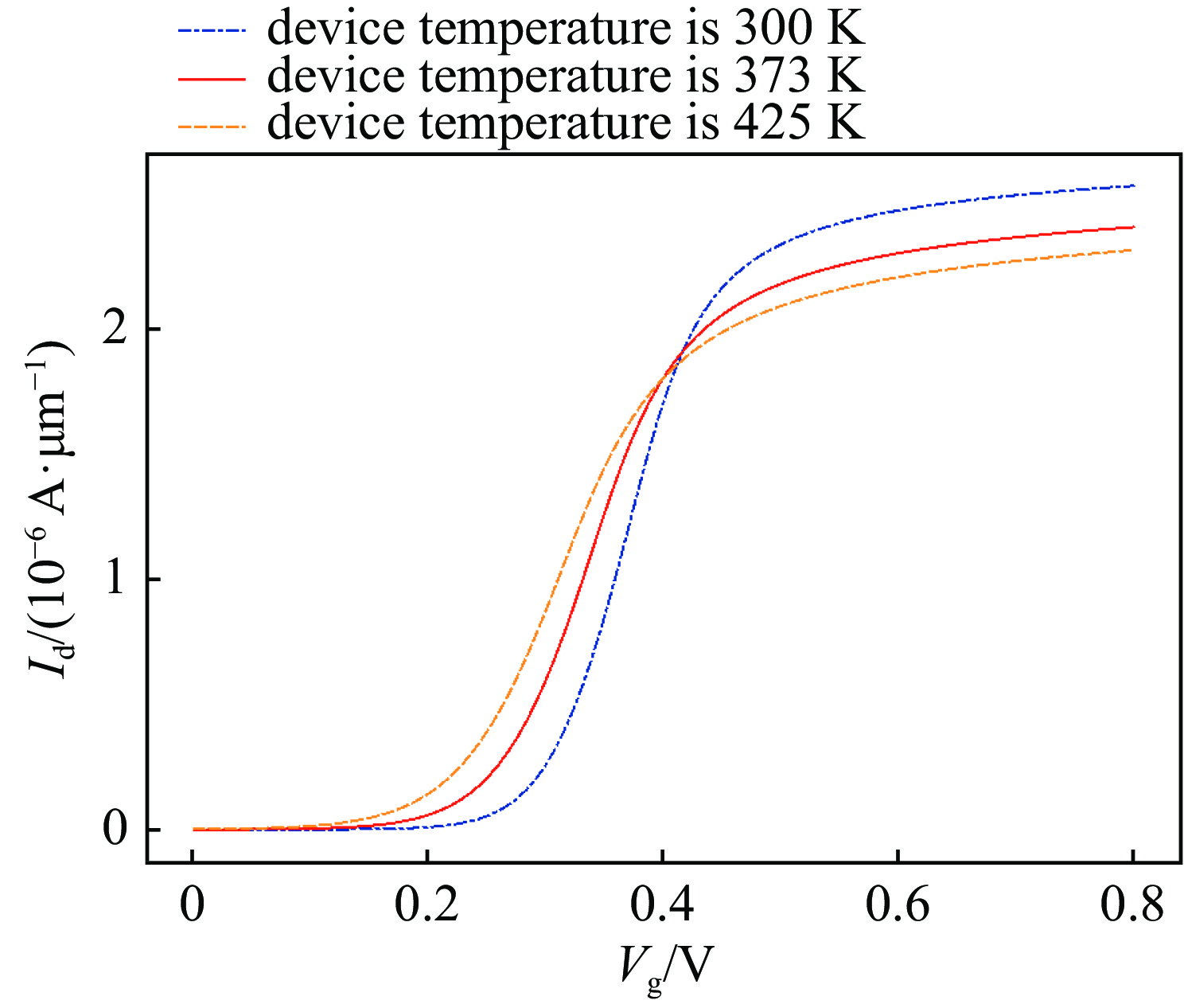
表 5 不同器件温度下VT、SS、DIBL
Table 5. VT, SS and DIBL under different device temperatures
device temperature/K VT/V SS/mV DIBL/(mV·V−1) 300 0.3041 67.6269 18.53 373 0.2620 86.6025 23.25 425 0.2282 101.2728 27.31
下载: 导出CSV
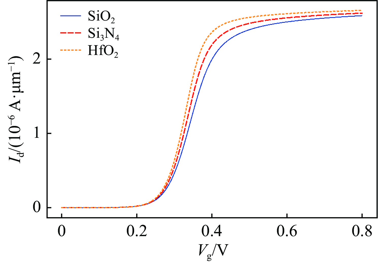
表 6 不同栅极材料下VT、SS、DIBL
Table 6. VT, SS and DIBL under different gate materials
gate materials gmax/mS SS/mV VT/V DIBL/(mV·V−1) SiO2 8.87×10⁻⁶ 65.34 0.2811 22.3 Si3N4 9.19×10⁻⁶ 64.81 0.2722 18.4 HfO2 9.54×10⁻⁶ 64.39 0.2736 6.4
下载: 导出CSV
-
[1] 缪晔辰. 鳍式场效应晶体管的有利特性及目前的研究方向[J]. 科技视界, 2021(15): 98-99Miao Yechen. The advantages of fin FET and the current research direction[J]. Science & Technology Vision, 2021(15): 98-99) [2] Hisamoto D, Lee W C, Kedzierski J, et al. FinFET—a self-aligned double-gate MOSFET scalable to 20 nm[J]. IEEE Transactions on Electron Devices, 2000, 47(12): 2320-2325. doi: 10.1109/16.887014 [3] 马伟彬. FinFET器件技术简介[J]. 科技展望, 2016, 26(16):104-105Ma Weibin. Introduction to FinFET device technology[J]. Science and Technology, 2016, 26(16): 104-105 [4] 单婵. 无结FinFET器件三维仿真研究[D]. 哈尔滨: 哈尔滨工程大学, 2014: 26-30Shan Chan. Three dimensional simulation of junctionless FinFET[D]. Harbin: Harbin Engineering University, 2014: 26-30 [5] Gaynor B D, Hassoun S. Fin shape impact on FinFET leakage with application to multithreshold and ultralow-leakage FinFET design[J]. IEEE Transactions on Electron Devices, 2014, 61(8): 2738-2744. doi: 10.1109/TED.2014.2331190 [6] Falk H. Prolog to: leakage current mechanisms and leakage reduction techniques in deep-submicrometer CMOS circuits[J]. Proceedings of the IEEE, 2003, 91(2): 303-304. doi: 10.1109/JPROC.2003.808154 [7] 李亚鹏, 李颖峰, 贺志荣, 等. 金属与半导体肖特基接触势垒模型及其载流子传输机制的研究进展[J]. 材料导报, 2017, 31(3):57-62Li Yapeng, Li Yingfeng, He Zhirong, et al. Progress of Schottky contact model and carrier transport mechanism at the interface between metal and semiconductor[J]. Materials Reports, 2017, 31(3): 57-62 [8] Al Imam S. Simulation of a 2D pn junction in silicon thin film incorporating quantum transport for carriers[D]. Montreal: Concordia University, 2006. [9] Appel J. Electron-electron scattering and transport phenomena in nonpolar semiconductors[J]. Physical Review, 1961, 122(6): 1760-1772. doi: 10.1103/PhysRev.122.1760 [10] Chen K J, Häberlen O, Lidow A, et al. GaN-on-Si power technology: devices and applications[J]. IEEE Transactions on Electron Devices, 2017, 64(3): 779-795. doi: 10.1109/TED.2017.2657579 [11] Boukortt N E I, Lenka T R, Patanè S, et al. Effects of varying the fin width, fin height, gate dielectric material, and gate length on the DC and RF performance of a 14-nm SOI FinFET structure[J]. Electronics, 2022, 11: 91. [12] 胡从振. SOI FinFET辐射效应研究[D]. 西安: 西安电子科技大学, 2019: 42Hu Congzhen. Study on reliability of irradiation effect of SOI FinFET[D]. Xi’an: Xidian University, 2019: 42 [13] 吕英波. 声子散射对载流子输运特性的影响[J]. 大学物理, 2017, 36(12):10-14Lv Yingbo. Effect of phonon scattering on carrier transport characteristics[J]. College Physics, 2017, 36(12): 10-14 [14] Taur Y, Ning T H. Fundamentals of modern VLSI devices[M]. New York: Cambridge University Press, 1998. [15] Choi J H, Murthy J, Roy K. The effect of process variation on device temperature in FinFET circuits[C]. 2007 IEEE/ACM International Conference on Computer-Aided Design. 2007: 747-751. [16] Venkateswarlu S, Sudarsanan A, Singh S G, et al. Ambient temperature-induced device self-heating effects on multi-Fin Si n-FinFET performance[J]. IEEE Transactions on Electron Devices, 2018, 65(7): 2721-2728. doi: 10.1109/TED.2018.2834979 [17] 曾庆王, 许会芳. 一种新型双材料双栅的MOSFET器件的性能研究[J]. 安徽理工大学学报(自然科学版), 2021, 41(6):61-66Zeng Qingwang, Xu Huifang. Research on the performance of a novel dual material double gate MOSFET[J]. Journal of Anhui University of Science and Technology (Natural Science), 2021, 41(6): 61-66 [18] Yin Longxiang, Du Gang, Liu Xiaoyan. Impact of ambient temperature on the self-heating effects in FinFETs[J]. Journal of Semiconductors, 2018, 39: 094011. doi: 10.1088/1674-4926/39/9/094011 [19] 黄宁, 刘伟景, 李清华, 等. 多栅FinFET性能研究及参数优化[J]. 电子工业专用设备, 2019, 48(5):61-67Huang Ning, Liu Weijing, Li Qinghua, et al. Research and optimization on multi-gate FinFET[J]. Equipment for Electronic Products Manufacturing, 2019, 48(5): 61-67 -

 点击查看大图
计量
- 文章访问数: 993
- HTML全文浏览量: 224
- PDF下载量: 114
- 被引次数: 0
