| Citation: | Liang Qishuai, Chai Changchun, Wu Han, et al. Damage characteristics and physical mechanism of the CMOS inverter under fast-rising-edge electromagnetic pulse[J]. High Power Laser and Particle Beams, 2022, 34: 083002. doi: 10.11884/HPLPB202234.220019

|
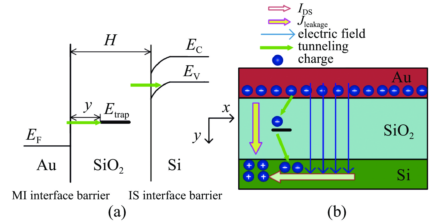
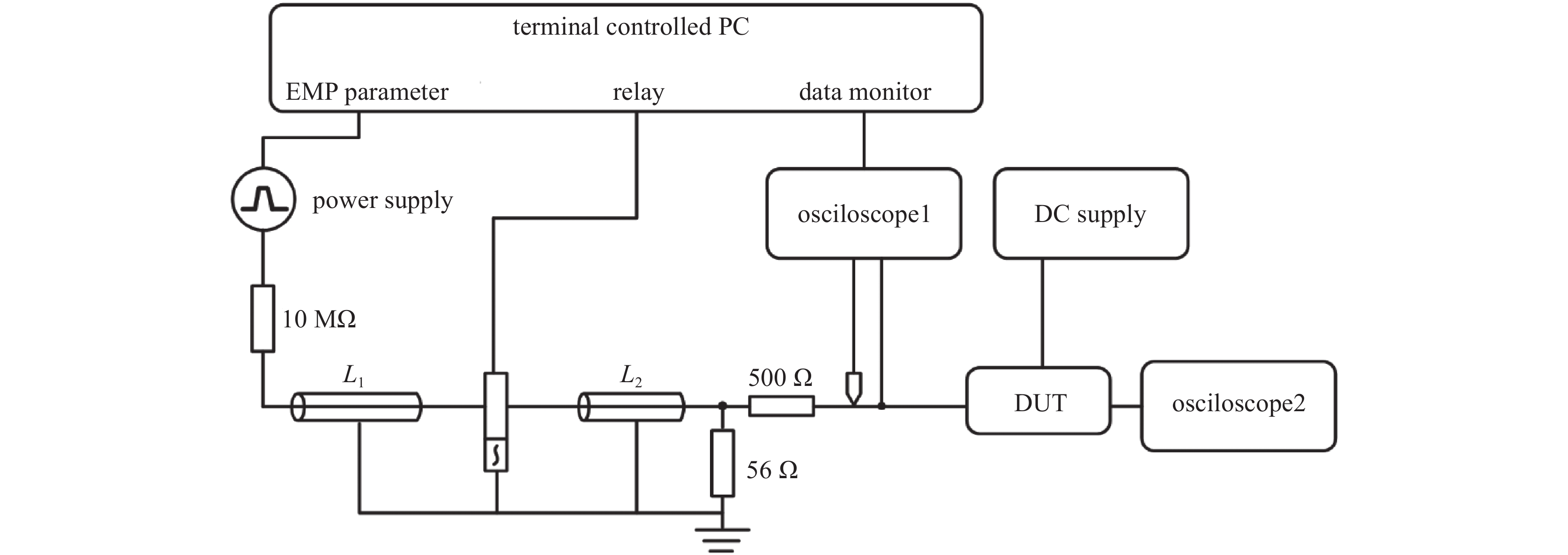
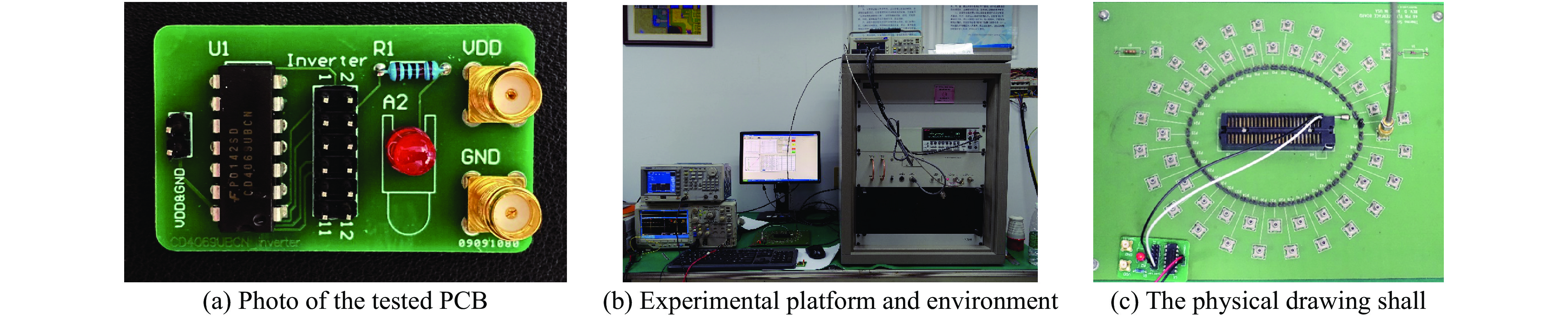
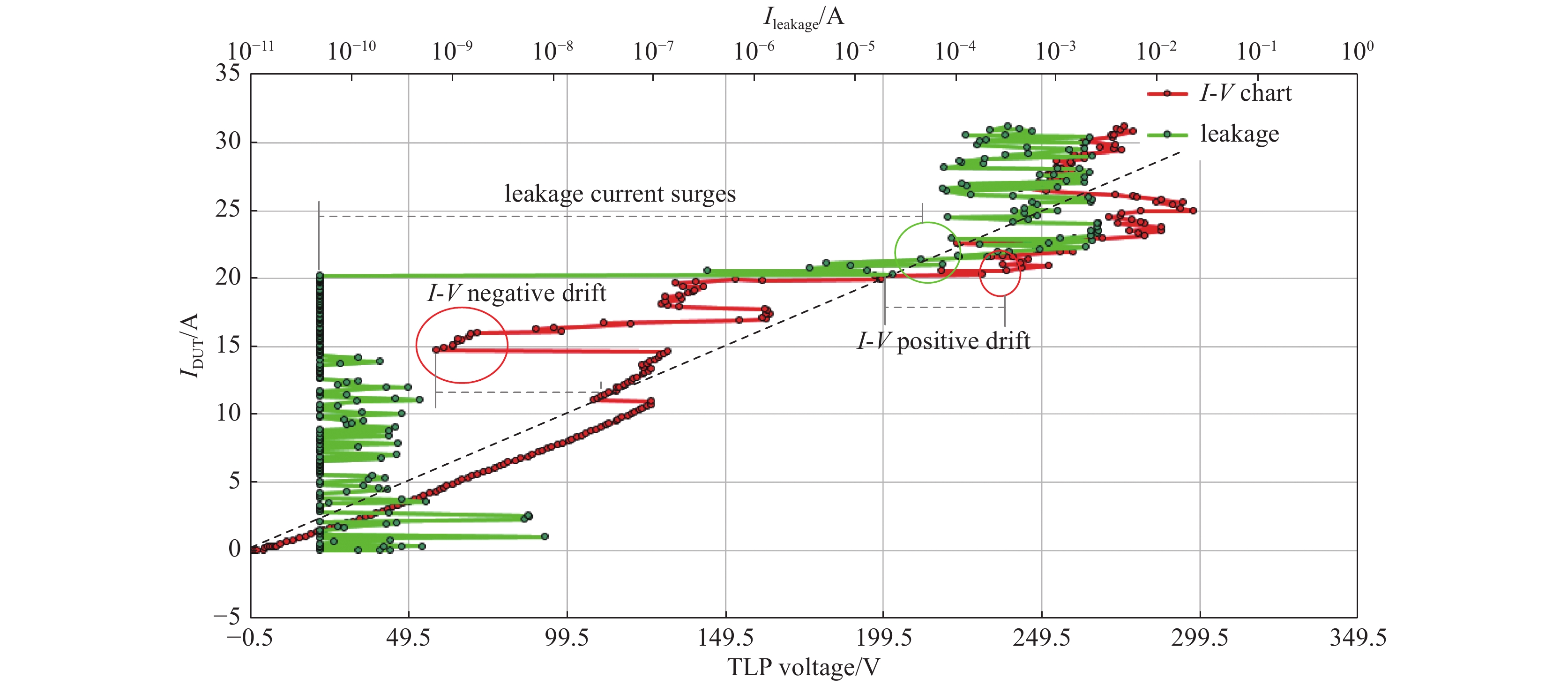
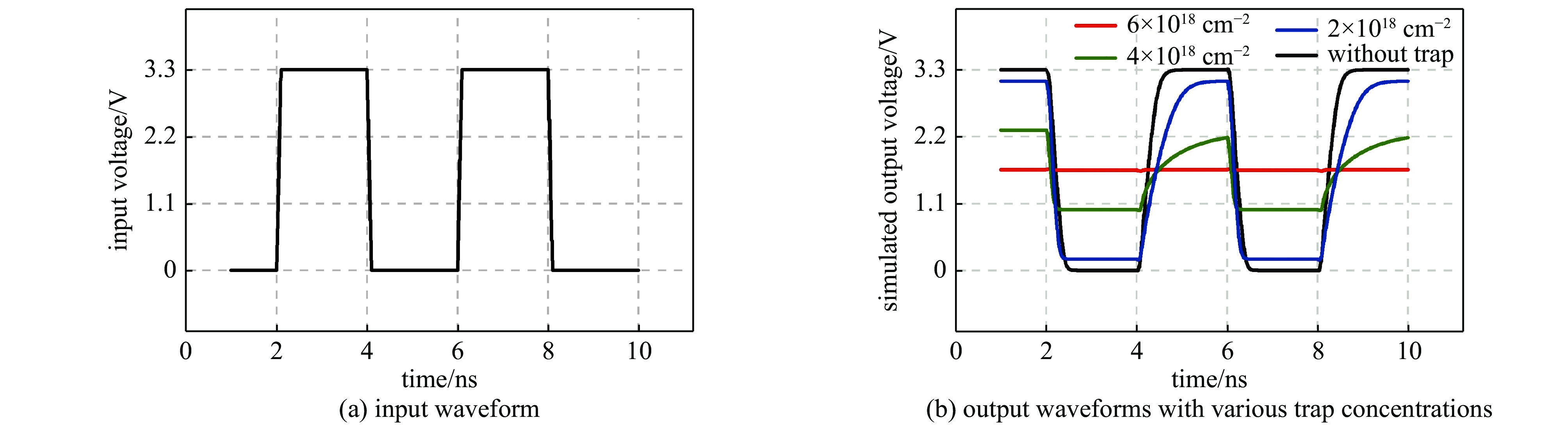
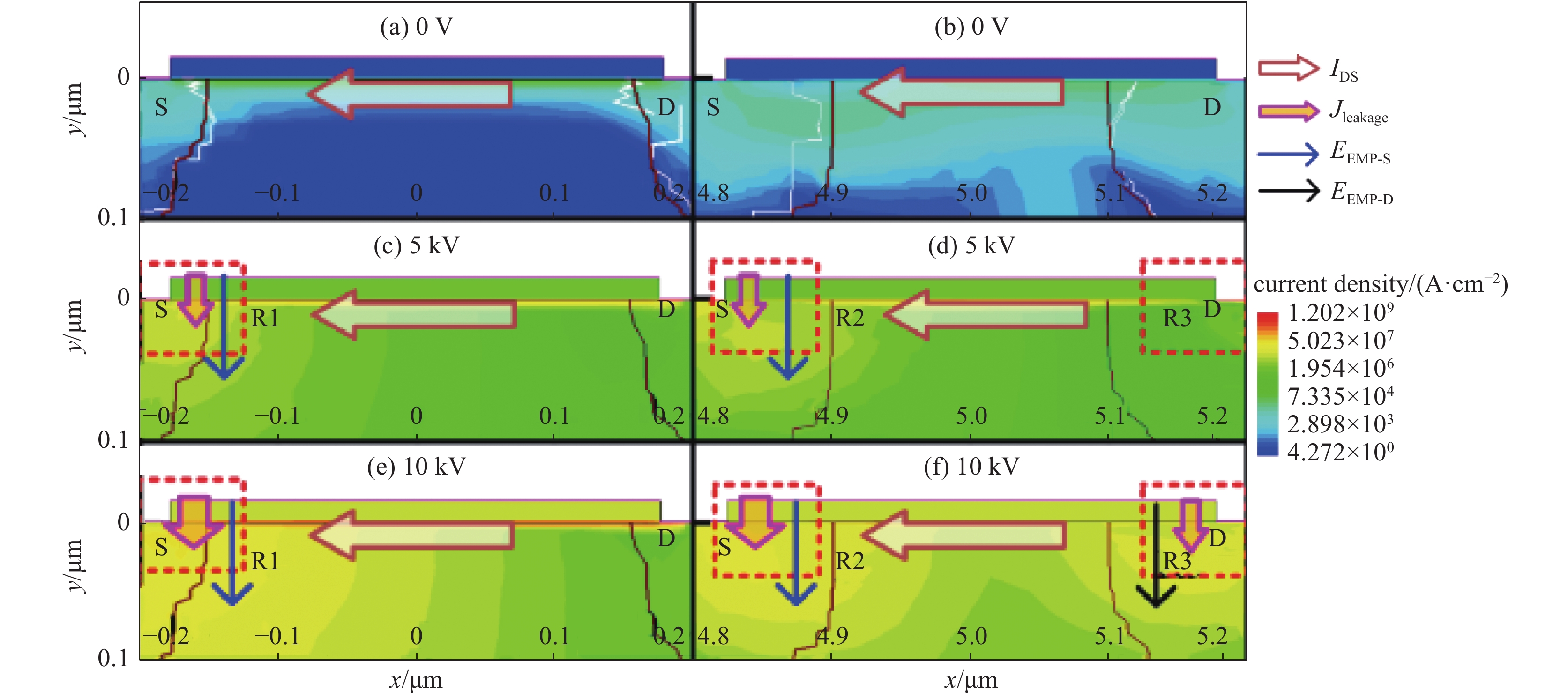
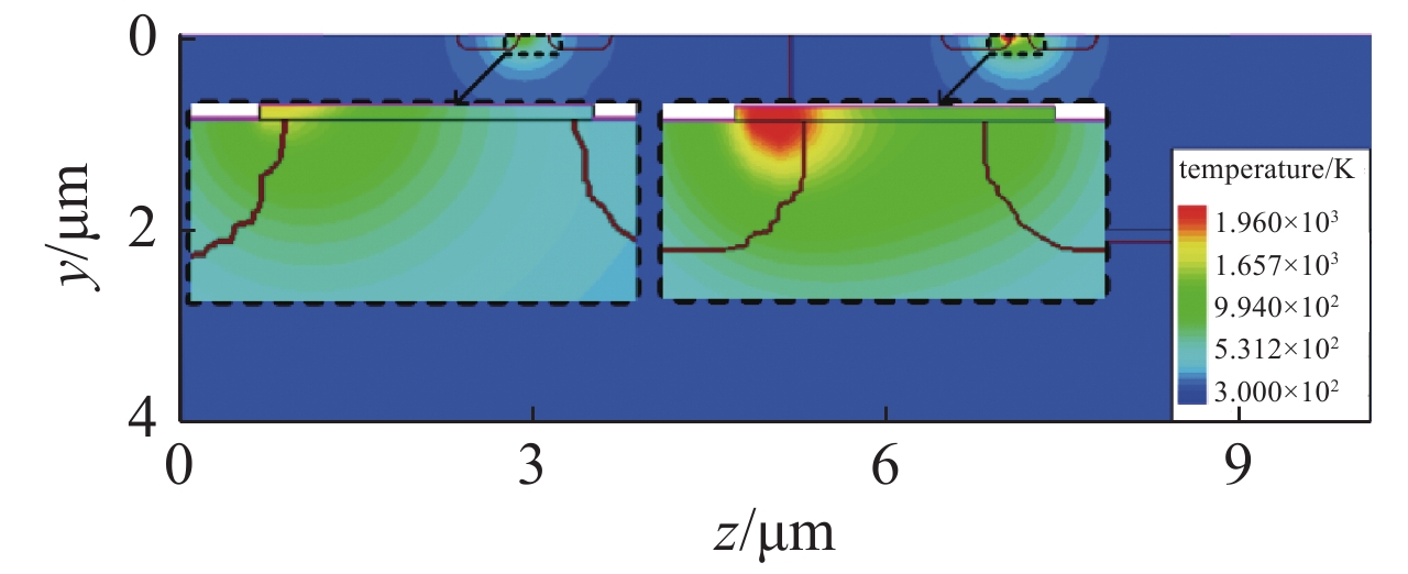
Ensuring the reliability of integrated circuits (ICs) has been a great challenge with the increasing complexity of the electromagnetic environment. On this basis, the fast-rising-edge electromagnetic pulse (EMP)-induced trap-assisted tunneling (TAT) effect is investigated by simulation and experiments of CMOS digital inverters. A detailed mechanism analysis is performed to explain the physical damage process. The EMP-induced field derives traps and leakage current in the oxide, which induces output degradation and thermal failure in the device. A theoretical model of degradation and failure is established to describe the dependency of the output deterioration and the heat accumulation on the EMP resulting signal features. The temperature distribution function is derived from the heat conduction equation in the semiconductor. Corresponding experiments performed based on the TLP test system substantiate the emerging performance deterioration, which is in agreement with the mechanism analysis. Simulated results from the Sentaurus TCAD indicate that EMP resulting voltage-induced damage is caused by the TAT current path occurring in the gate oxide, revealing the location susceptible to burnout. In addition, the dependency of the device failure on the pulse rising time is discussed. The mechanism analysis in this paper facilitates reinforcing the design and promotes EMP reliability research on other semiconductor devices, and the study contributes to the enhancement of EMP robustness in CMOS digital ICs.

| [1] |
Brauer F, Sabath F, ter Haseborg J L. Susceptibility of IT network systems to interferences by HPEM[C]//Proceedings of 2009 IEEE International Symposium on Electromagnetic Compatibility. IEEE, 2009: 137.
|
| [2] |
Klünder C, ter Haseborg J T. Effects of high-power and transient disturbances on wireless communication systems operating inside the 2.4 GHz ISM band[C]//Proceedings of 2010 IEEE International Symposium on Electromagnetic Compatibility. IEEE, 2010: 359-363.
|
| [3] |
Nitsch D, Camp M, Sabath F, et al. Susceptibility of some electronic equipment to HPEM threats[J]. IEEE Transactions on Electromagnetic Compatibility, 2004, 46(3): 380-389. doi: 10.1109/TEMC.2004.831842
|
| [4] |
Månsson D, Thottappillil R, Nilsson T, et al. Susceptibility of civilian GPS receivers to electromagnetic radiation[J]. IEEE Transactions on Electromagnetic Compatibility, 2008, 50(2): 434-437. doi: 10.1109/TEMC.2008.921015
|
| [5] |
Wu Jie, Rosenbaum E. Gate oxide reliability under ESD-like pulse stress[J]. IEEE Transactions on Electron Devices, 2004, 51(9): 1192-1196.
|
| [6] |
Greetsai V N, Kozlovsky A H, Kuvshinnikov V M, et al. Response of long lines to nuclear high-altitude electromagnetic pulse (HEMP)[J]. IEEE Transactions on Electromagnetic Compatibility, 1998, 40(4): 348-354. doi: 10.1109/15.736221
|
| [7] |
Chahine I, Kadi M, Gaboriaud E, et al. Characterization and modeling of the susceptibility of integrated circuits to conducted electromagnetic disturbances Up to 1 GHz[J]. IEEE Transactions on Electromagnetic Compatibility, 2008, 50(2): 285-293. doi: 10.1109/TEMC.2008.918983
|
| [8] |
Kim K, Iliadis A A. Impact of microwave interference on dynamic operation and power dissipation of CMOS inverters[J]. IEEE Transactions on Electromagnetic Compatibility, 2007, 49(2): 329-338. doi: 10.1109/TEMC.2007.893333
|
| [9] |
Kim K, Iliadis A A. Critical bit errors in CMOS digital inverters due to pulsed electromagnetic interference[C]//Proceedings of 2007 International Conference on Electromagnetics in Advanced Applications. IEEE, 2007.
|
| [10] |
Iliadis A A, Kim K. Theoretical foundation for upsets in CMOS circuits due to high-power electromagnetic interference[J]. IEEE Transactions on Device and Materials Reliability, 2010, 10(3): 347-352. doi: 10.1109/TDMR.2010.2050692
|
| [11] |
You Hailong, Lan Jianchun, Fan Juping, et al. Research on characteristics degradation of n-metal-oxide-semiconductor field-effect transistor induced by hot carrier effect due to high power microwave[J]. Acta Physica Sinica, 2012, 61: 108501. doi: 10.7498/aps.61.108501
|
| [12] |
Korte S, Camp M, Garbe H. Hardware and software simulation of transient pulse impact on integrated circuits[C]//Proceedings of 2005 International Symposium on Electromagnetic Compatibility. IEEE, 2005.
|
| [13] |
Camp M, Korte S, Garbe H. Classification of the destruction effects in CMOS-devices after impact of fast transient electromagnetic pulses[M]//Sabath F, Mokole E L, Schenk U, et al. Ultra-wideband, short-pulse electromagnetics 7. New York: Springer, 2007.
|
| [14] |
Wang Haiyang, Li Jiayin, Li Hao, et al. Experimental study and SPICE simulation of CMOS inverters LATCH-Up effects due to high power microwave interference[J]. Progress in Electromagnetics Research, 2008, 87: 313-330. doi: 10.2528/PIER08100408
|
| [15] |
Wang Haiyang, Hu Fei, Hu Biao, et al. Characteristics of microwave breakdown in cavity filter under high power microwave environment[C]//Proceedings of 2020 IEEE MTT-S International Conference on Numerical Electromagnetic and Multiphysics Modeling and Optimization (NEMO). IEEE, 2020.
|
| [16] |
Zhang Yuhang, Chai Changchun, Liu Yang, et al. Modeling and understanding of the thermal failure induced by high power microwave in CMOS inverter[J]. Chinese Physics B, 2017, 26: 058502. doi: 10.1088/1674-1056/26/5/058502
|
| [17] |
Liang Qishuai, Chai Changchun, Wu Han, et al. Mechanism analysis and thermal damage prediction of high-power microwave radiated CMOS circuits[J]. IEEE Transactions on Device and Materials Reliability, 2021, 21(3): 444-451. doi: 10.1109/TDMR.2021.3104760
|
| [18] |
Liu Yuqian, Chai Changchun, Zhang Yuhang, et al. Physics-based analysis and simulation model of electromagnetic interference induced soft logic upset in CMOS inverter[J]. Chinese Physics B, 2018, 27: 068505. doi: 10.1088/1674-1056/27/6/068505
|
| [19] |
Chen Jie, Du Zhengwei. Device simulation studies on latch-up effects in CMOS inverters induced by microwave pulse[J]. Microelectronics Reliability, 2013, 53(3): 371-378. doi: 10.1016/j.microrel.2012.10.012
|
| [20] |
Liu Yuqian, Chai Changchun, Wu Han, et al. Mechanism of AlGaAs/InGaAs pHEMT nonlinear response under high-power microwave radiation[J]. IEEE Journal of the Electron Devices Society, 2020, 8: 731-737. doi: 10.1109/JEDS.2020.3008816
|
| [21] |
Zhou Liang, San Zhengwei, Hua Yujie, et al. Investigation on failure mechanisms of GaN HEMT caused by high-power microwave (HPM) pulses[J]. IEEE Transactions on Electromagnetic Compatibility, 2017, 59(3): 902-909. doi: 10.1109/TEMC.2016.2628046
|
| [22] |
Chai Changchun, Ma Zhenyang, Ren Xingrong, et al. Hardening measures for bipolar transistors against microwave-induced damage[J]. Chinese Physics B, 2013, 22: 068502. doi: 10.1088/1674-1056/22/6/068502
|
| [23] |
Liu Yang, Chai Changchun, Yu Xinhai, et al. Damage effects and mechanism of the GaN high electron mobility transistor caused by high electromagnetic pulse[J]. Acta Physica Sinica, 2016, 65: 038402. doi: 10.7498/aps.65.038402
|
| [24] |
Xi Xiaowen, Chai Changchun, Zhao Gang, et al. Damage effect and mechanism of the GaAs pseudomorphic high electron mobility transistor induced by the electromagnetic pulse[J]. Chinese Physics B, 2016, 25: 048503. doi: 10.1088/1674-1056/25/4/048503
|
| [25] |
Xi Xiaowen, Chai Changchun, Liu Yang, et al. Analysis of the damage threshold of the GaAs pseudomorphic high electron mobility transistor induced by the electromagnetic pulse[J]. Chinese Physics B, 2016, 25: 088504. doi: 10.1088/1674-1056/25/8/088504
|
| [26] |
Kim K C. High power microwave interference effects on analog and digital circuits in IC’s[D]. Washington, DC: University of Maryland, 2007: 117-130.
|
| [27] |
Zhi Jiang, Zhuang Yiqi, Li Cong, et al. Influence of trap-assisted tunneling on trap-assisted tunneling current in double gate tunnel field-effect transistor[J]. Chinese Physics B, 2016, 25: 027701. doi: 10.1088/1674-1056/25/2/027701
|
| [28] |
Radasky W A, Baum C E, Wik M W. Introduction to the special issue on high-power electromagnetics (HPEM) and intentional electromagnetic interference (IEMI)[J]. IEEE Transactions on Electromagnetic Compatibility, 2004, 46(3): 314-321. doi: 10.1109/TEMC.2004.831899
|
| [29] |
Khairurrijal, Noor F A, Sukirno. Modeling of stress-induced leakage current in thin gate oxides[C]. Proceedings of the 9th International Conference on Neural Information Processing. Computational Intelligence for the E-Age. 2002.
|
Figures(10)


 DownLoad: