

Design of electron gun for electron beam irradiation of vertical graphene
-
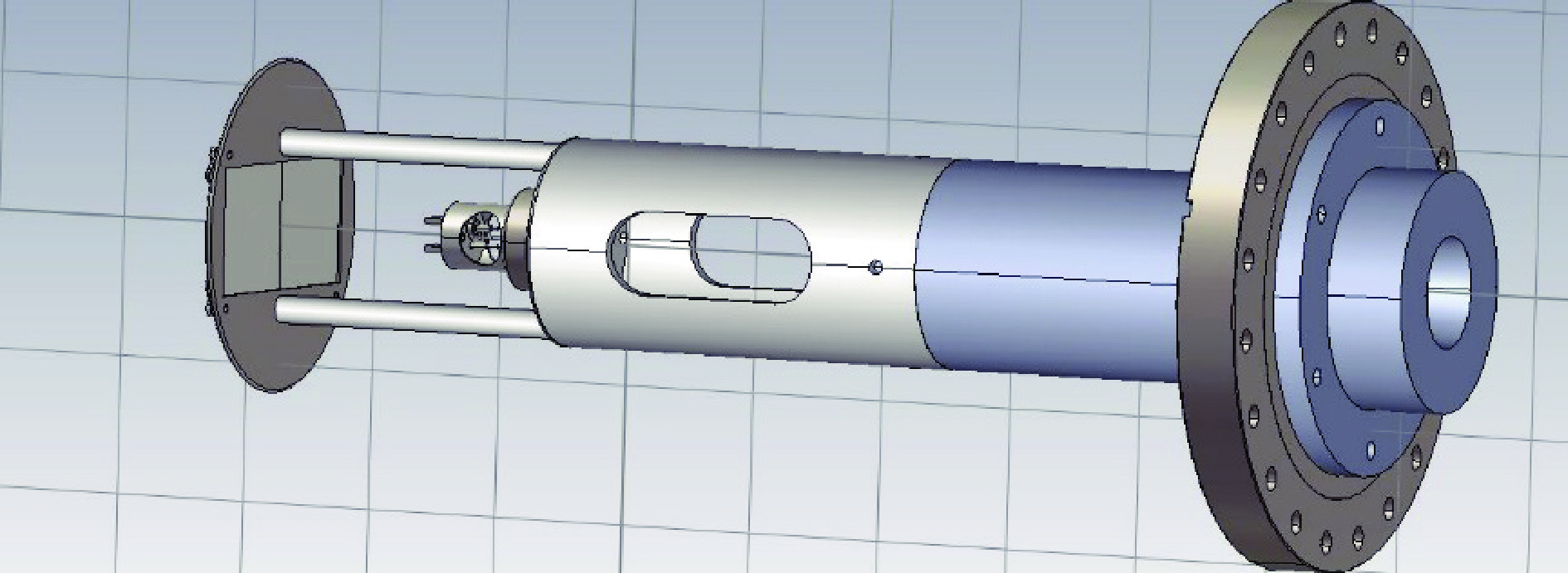
摘要: 多项研究表明,材料表面的立式石墨烯涂层能够显著降低二次电子产额,且二次电子产额最大值所对应的入射电子能量通常在百电子伏特。在电子束辐照的实际工况下,立式石墨烯的微观结构会经历复杂的动态演变过程,这些微观结构变化的方式、特点以及由其导致的二次电子发射特性的变化程度与机理可能各不相同。为系统研究电子束辐照参数对立式石墨烯微观结构演变及其二次电子发射特性的影响规律,本研究采用理论仿真与实验验证相结合的研究方法,自主设计并研制了一套专门用于立式石墨烯辐照研究的电子束辐照系统。Abstract: Numerous studies have demonstrated that vertical graphene coatings on material surfaces can significantly reduce the secondary electron yield, with the maximum secondary electron yield typically occurring at incident electron energies in the range of hundreds of electron volts. Under actual electron beam irradiation conditions, the microstructure of vertical graphene undergoes complex dynamic evolution processes. These structural changes exhibit diverse characteristic patterns, leading to varying degrees of alteration in secondary electron emission properties, with distinct underlying mechanisms. To systematically investigate the influence of electron beam irradiation parameters on the microstructural evolution of vertical graphene and its secondary electron emission characteristics, employing a combined approach of theoretical simulation and experimental verification, this study has independently designed and developed a dedicated electron beam irradiation system specifically for vertical graphene research.
-
Key words:
- electron beam irradiation /
- electron gun /
- hot cathode /
- beam spot test /
- vertical graphene
-
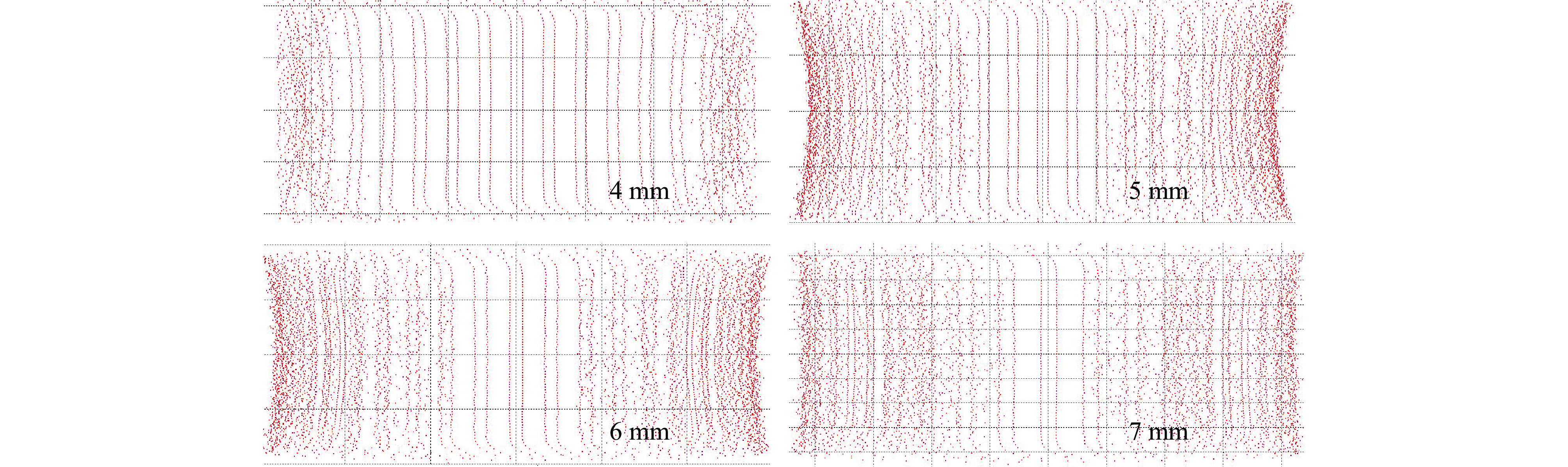
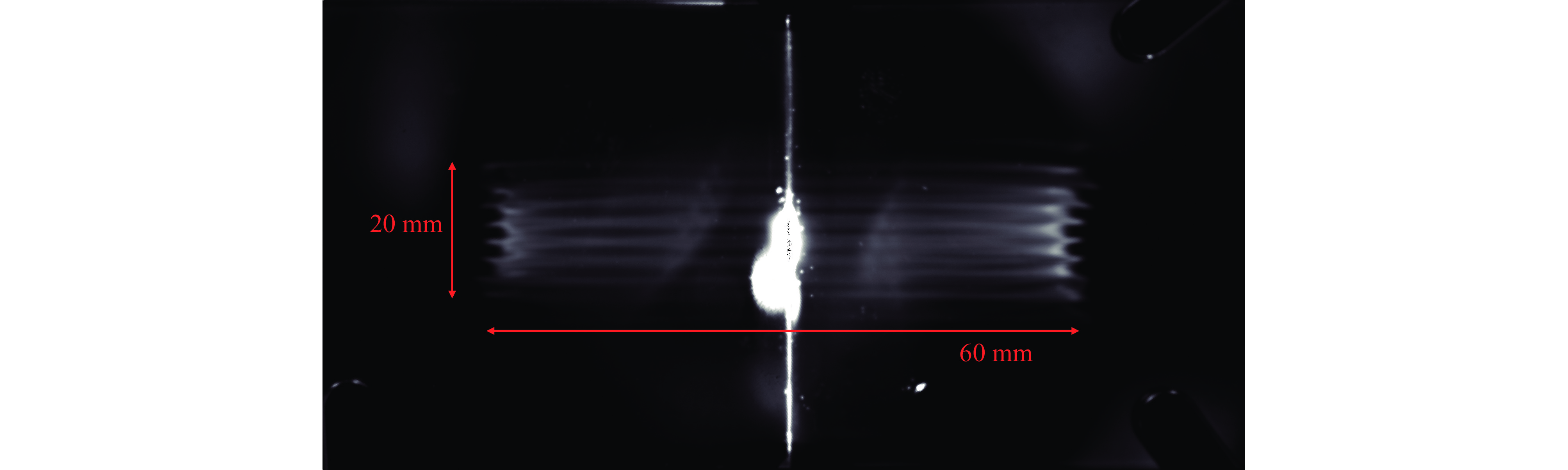
图 5 聚焦极高度为4 mm、5 mm、6 mm、7 mm的束斑结果
Figure 5. Beam spot results for focusing pole heights of 4 mm, 5 mm, 6 mm, and 7 mm
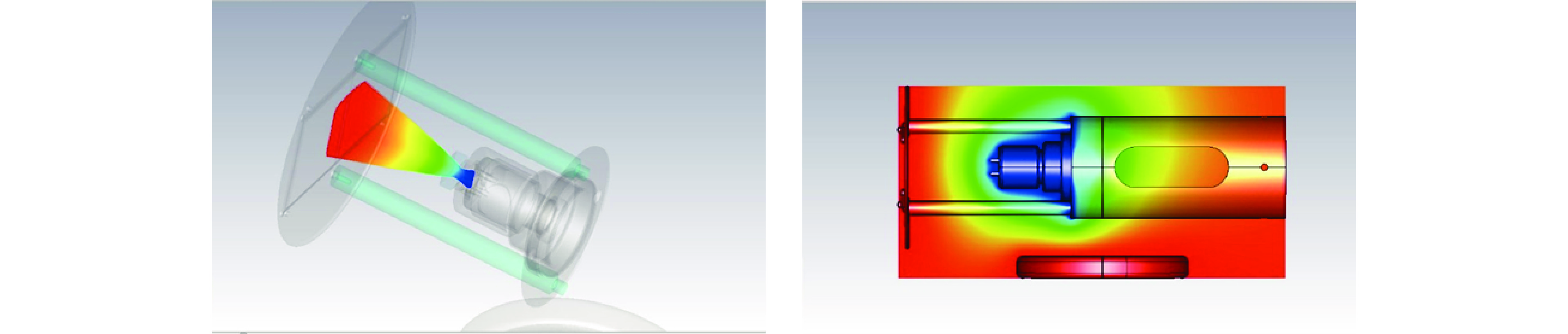
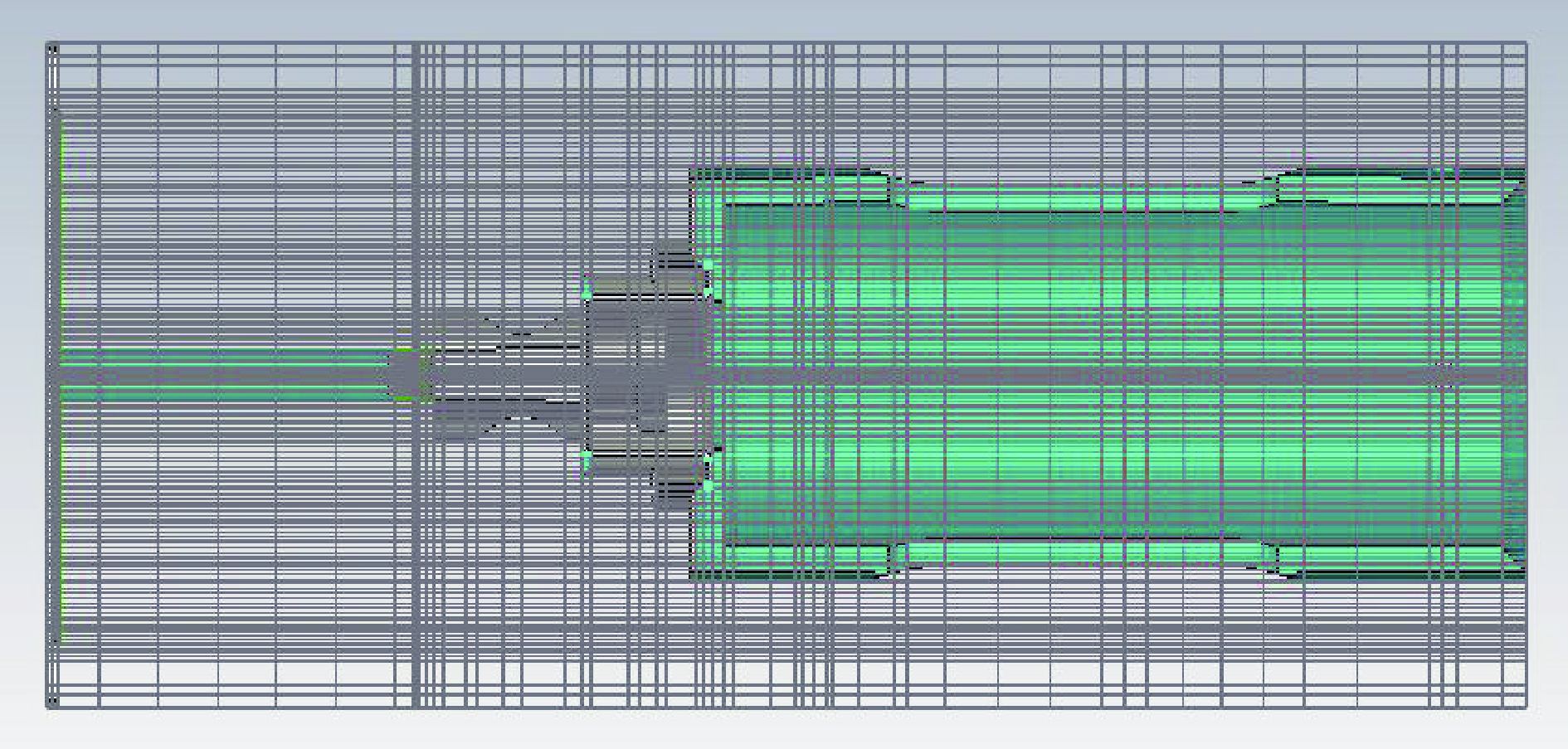
图 6 电子束轨迹和电子枪的等势面
Figure 6. Electron beam trajectory and isopotential surface of the electron gun
-
[1] Cimino R, Collins I R, Furman M A, et al. Can low-energy electrons affect high-energy physics accelerators?[J]. Physical Review Letters, 2004, 93: 014801. doi: 10.1103/PhysRevLett.93.014801 [2] 何佳龙, 陈思富, 张篁, 等. 神龙二号加速器绝缘环真空沿面闪络[J]. 强激光与粒子束, 2016, 28:095101 doi: 10.11884/HPLPB201628.150950He Jialong, Chen Sifu, Zhang Huang, et al. Vacuum flashover of Dragon-Ⅱ accelerator insulator ring[J]. High Power Laser and Particle Beams, 2016, 28: 095101 doi: 10.11884/HPLPB201628.150950 [3] Ecoffet R. Overview of In-orbit radiation induced spacecraft anomalies[J]. IEEE Transactions on Nuclear Science, 2013, 60(3): 1791-1815. [4] 何友辉, 陈洪斌, 李飞, 等. 固体绝缘子的真空沿面闪络研究[J]. 强激光与粒子束, 2023, 35:035004 doi: 10.11884/HPLPB202335.220214He Youhui, Chen Hongbin, Li Fei, et al. Review of surface flashover and surface charge behavior of vacuum insulators[J]. High Power Laser and Particle Beams, 2023, 35: 035004 doi: 10.11884/HPLPB202335.220214 [5] Montero I, Aguilera L, Dávila M E, et al. Secondary electron emission under electron bombardment from graphene nanoplatelets[J]. Applied Surface Science, 2014, 291: 74-77. [6] He Jialong, Yang Jie, Peng Yufei, et al. Measurement of yield and spectrum of secondary electron emission and their characteristics under modification of conductive materials[J]. Review of Scientific Instruments, 2019, 90: 063304. [7] Lee S W, Baik Y J, Kang C J, et al. Suppression of secondary electrons from diamond by whisker formation[J]. Applied Surface Science, 2003, 215(1/4): 265-268. [8] Patino M, Raitses Y, Wirz R. Secondary electron emission from plasma-generated nanostructured tungsten fuzz[J]. Applied Physics Letters, 2016, 109: 201602. [9] Zhou Yangbo, Jadwiszczak J, Keane D, et al. Programmable graphene doping via electron beam irradiation[J]. Nanoscale, 2017, 9(25): 8657-8664. [10] Teweldebrhan D, Balandin A A. Modification of graphene properties due to electron-beam irradiation[J]. Applied Physics Letters, 2009, 94: 013101. doi: 10.1063/1.3062851 [11] Childres I, Jauregui L A, Foxe M, et al. Effect of electron-beam irradiation on graphene field effect devices[J]. Applied Physics Letters, 2010, 97: 173109. doi: 10.1063/1.3502610 [12] Hossain Z, Rumyantsev S, Shur M S, et al. Reduction of 1/f noise in graphene after electron-beam irradiation[J]. Applied Physics Letters, 2013, 102: 153512. doi: 10.1063/1.4802759 [13] Liu Guanxiong, Teweldebrhan D, Balandin A A. Tuning of graphene properties via controlled exposure to electron beams[J]. IEEE Transactions on Nanotechnology, 2011, 10(4): 865-870. doi: 10.1109/TNANO.2010.2087391 [14] Kim H, Park W, Nam K, et al. Effects of electron beam irradiation on the friction and work function of the wrinkled graphene[J]. Current Applied Physics, 2019, 19(11): 1172-1176. doi: 10.1016/j.cap.2019.07.013 [15] He Y H, Wang L, Chen X L, et al. Modifying electronic transport properties of graphene by electron beam irradiation[J]. Applied Physics Letters, 2011, 99: 033109. doi: 10.1063/1.3615294 [16] Thiele C, Felten A, Echtermeyer T J, et al. Electron-beam-induced direct etching of graphene[J]. Carbon, 2013, 64: 84-91. doi: 10.1016/j.carbon.2013.07.038 -

 下载:
下载:
 点击查看大图
图(9)
计量
- 文章访问数: 100
- HTML全文浏览量: 31
- PDF下载量: 14
- 被引次数: 0
