| Citation: | Wang Yuting, Chen Mengqi, Ju Xin. Applications of neutron diffraction in semiconductor materials and devices research[J]. High Power Laser and Particle Beams. doi: 10.11884/HPLPB202537.250212

|

| [1] |
Woracek R, Santisteban J, Fedrigo A, et al. Diffraction in neutron imaging—A review[J]. Nuclear Instruments and Methods in Physics Research Section A: Accelerators, Spectrometers, Detectors and Associated Equipment, 2018, 878: 141-158.
|
| [2] |
林皓, 李建, 杨钊龙, 等. 中子衍射应力分析技术及其应用进展[J]. 金属学报, 2024, 60(8): 1017-1030 doi: 10.11900/0412.1961.2024.00061
Lin Hao, Li Jian, Yang Zhaolong, et al. Recent progress in stress analysis technology and application of neutron diffraction[J]. Acta Metallurgica Sinica, 2024, 60(8): 1017-1030 doi: 10.11900/0412.1961.2024.00061
|
| [3] |
郑海彪, 康乐, 陈洁, 等. 多场耦合原位拉伸中子衍射实验装置综述[J]. 强激光与粒子束, 2024, 36: 106002 doi: 10.11884/HPLPB202436.240207
Zheng Haibiao, Kang Le, Chen Jie, et al. A review of multi-field coupled in-situ stretching neutron diffraction experimental devices[J]. High Power Laser and Particle Beams, 2024, 36: 106002 doi: 10.11884/HPLPB202436.240207
|
| [4] |
王立鹏, 孔令体, 姜夺玉, 等. 基于经典分子动力学模拟的热中子散射数据产生方法[J]. 现代应用物理, 2025, 16: 020203 doi: 10.12061/j.issn.2095-6223.202407039
Wang Lipeng, Kong Lingti, Jiang Duoyu, et al. Thermal neutron scattering data generation method based on classical molecular dynamics simulations[J]. Modern Applied Physics, 2025, 16: 020203 doi: 10.12061/j.issn.2095-6223.202407039
|
| [5] |
Roehrens D, Brendt J, Samuelis D, et al. On the ammonolysis of Ga2O3: an XRD, neutron diffraction and XAS investigation of the oxygen-rich part of the system Ga2O3–GaN[J]. Journal of Solid State Chemistry, 2010, 183(3): 532-541. doi: 10.1016/j.jssc.2009.12.024
|
| [6] |
Suehiro T, Tansho M, Hagihala M, et al. Quaternary nitride system (1−x)ZnGeN2−2xGaN (x = 1/3): disordered wurtzite structure revealed by time-of-flight neutron powder diffraction[J]. Applied Physics Express, 2020, 13: 115503. doi: 10.35848/1882-0786/abc1cb
|
| [7] |
Dong Liran, Zhang Jie, Li Yizhuang, et al. Borrowed dislocations for ductility in ceramics[J]. Science, 2024, 385(6707): 422-427. doi: 10.1126/science.adp0559
|
| [8] |
Dhanalakshmi Veeraraj M R, Qu Di, Zhao Shuai, et al. Diffractive lenses for neutron techniques[J]. Scientific Reports, 2025, 15: 8408. doi: 10.1038/s41598-025-92329-6
|
| [9] |
Martel P, Rogers D, Stephens A E. Neutron diffraction as a rapid screening method for semiconductor wafers[J]. Applied Physics Letters, 1987, 51(22): 1795-1797. doi: 10.1063/1.98525
|
| [10] |
谭志新, 敬罕涛, 樊瑞睿, 等. 中国散裂中子源伴生质子辐照实验平台及其技术参数的确定[J]. 现代应用物理, 2024, 15: 020401 doi: 10.12061/j.issn.2095-6223.2024.020401
Tan Zhixin, Jing Hantao, Fan Ruirui, et al. Associated protons experimental platform of China spallation neutron source and determination of its technical parameters[J]. Modern Applied Physics, 2024, 15: 020401 doi: 10.12061/j.issn.2095-6223.2024.020401
|
| [11] |
Wang Yanxu, Gong Wu, Kawasaki T, et al. In situ neutron diffraction study on the deformation behavior of the plastic inorganic semiconductor Ag2S[J]. Applied Physics Letters, 2023, 123: 011903. doi: 10.1063/5.0158607
|
| [12] |
Bokuchava G D. Materials microstructure characterization using high resolution time-of-flight neutron diffraction[J]. Romanian Journal of Physics, 2016, 61(5/6): 903-925.
|
| [13] |
Son B S, Kim S J, Lee B W, et al. Mössbauer spectroscopy and neutron diffraction studies of the ferrimagnetic semiconductor on Ga-substituted FeGaxCr2−xS4[J]. Journal of Applied Physics, 2005, 97: 10D322. doi: 10.1063/1.1854051
|
| [14] |
Wang Zhenyu, Breternitz J, Schorr S. Cation disorder in zinc-group IV- nitride and oxide nitride semiconductor materials revealed through neutron diffraction[J]. Acta Crystallographica Section A: Foundations and Advances, 2021, A77: C1077.
|
| [15] |
Hanada T, Izumi F, Nakamura Y, et al. Neutron and electron diffraction studies of ZnGa2Se4[J]. Physica B: Condensed Matter, 1997, 241/243: 373-375.
|
| [16] |
Rhyne J J, Lin J, Furdyna J K, et al. Anomalous antiferromagnetic coupling in [ZnTe¦MnTe] superlattices[J]. Journal of Magnetism and Magnetic Materials, 1998, 177/181: 1195-1196.
|
| [17] |
Vennix C W H M, Frikkee E, Swagten H J M, et al. Neutron diffraction on the diluted magnetic semiconductor Sn1−xMnxTe[J]. Journal of Applied Physics, 1991, 69(8): 6025-6027. doi: 10.1063/1.347805
|
| [18] |
Giebultowicz T M, Kepa H, Blinowski J, et al. Neutron diffraction and reflectivity studies of interlayer correlations in magnetic semiconductor superlattices[J]. Physica E: Low-Dimensional Systems and Nanostructures, 2001, 10(1/3): 411-418.
|
| [19] |
Goldman K I, Springholz G, Kepa H, et al. Interlayer correlations in antiferromagnetic semiconductor superlattices EuTe/PbTe[J]. Physica B: Condensed Matter, 1997, 241/243: 710-713.
|
| [20] |
Kȩpa H, Kutner-Pielaszek J, Twardowski A, et al. Interlayer correlations in ferromagnetic semiconductor superlattices EuS/PbS[J]. Journal of Magnetism and Magnetic Materials, 2001, 226/230: 1795-1797.
|
| [21] |
Dolling G, Holden T M, Sears V F, et al. Neutron diffraction studies of diluted magnetic semiconductors (invited)[J]. Journal of Applied Physics, 1982, 53(11): 7644-7648. doi: 10.1063/1.330174
|
| [22] |
Messenger G C. A summary review of displacement damage from high energy radiation in silicon semiconductors and semiconductor devices[J]. IEEE Transactions on Nuclear Science, 1992, 39(3): 468-473. doi: 10.1109/23.277547
|
| [23] |
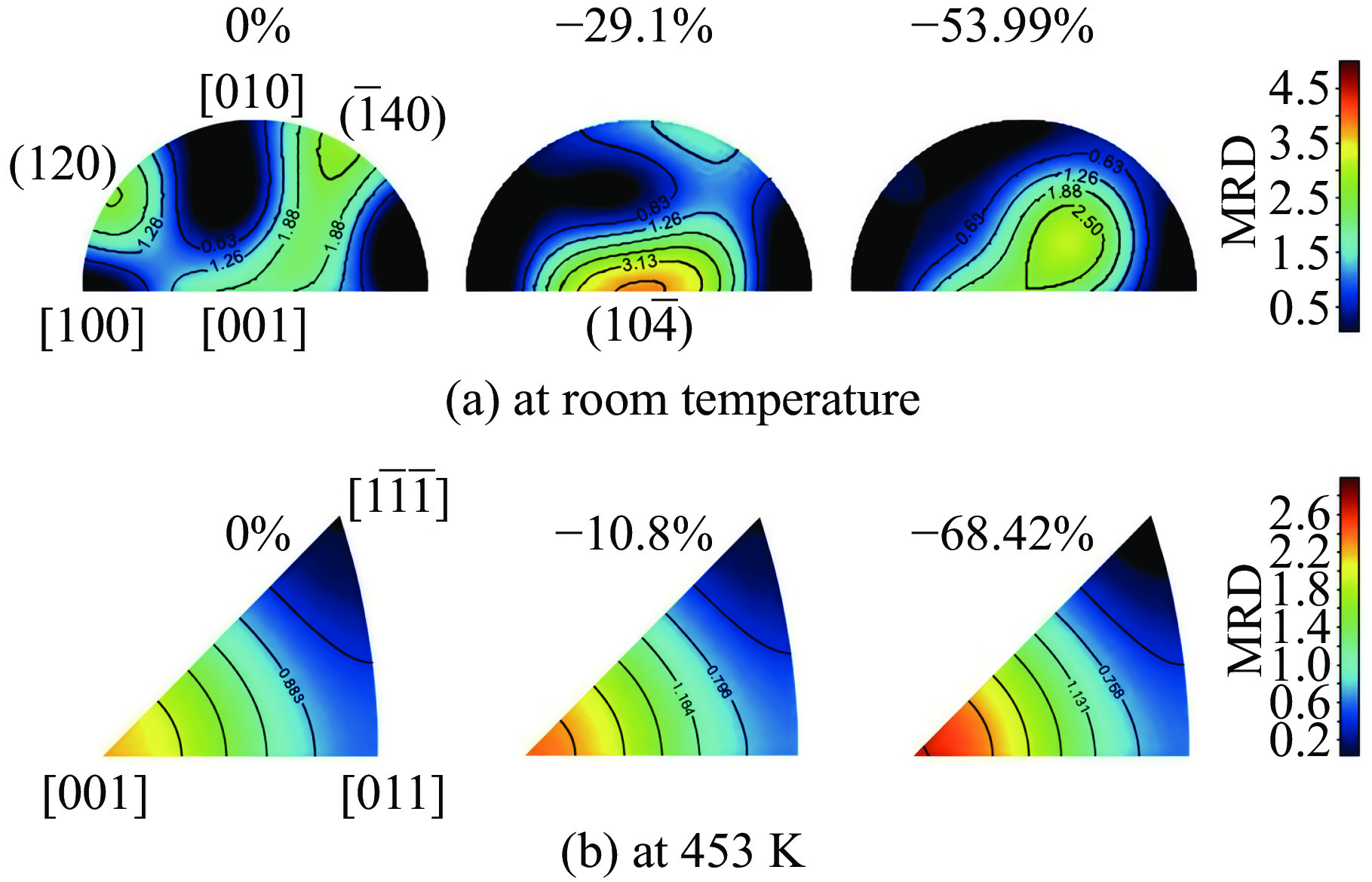
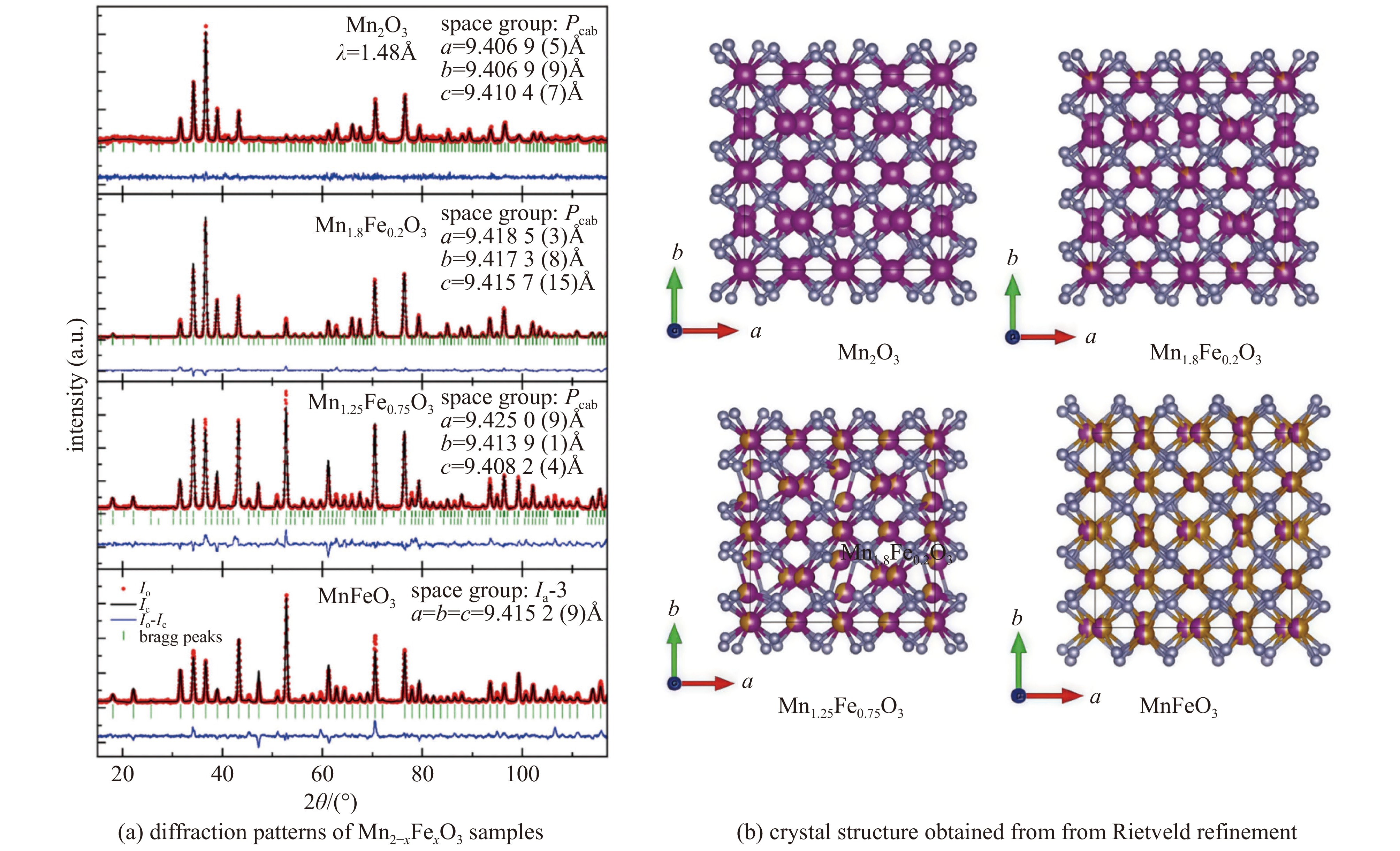
Nikam R, Kurawle N, Borole S, et al. Neutron diffraction studies of Fe-substituted Mn2O3[J]. Indian Journal of Physics, 2023, 97(9): 2721-2725. doi: 10.1007/s12648-023-02621-2
|
| [24] |
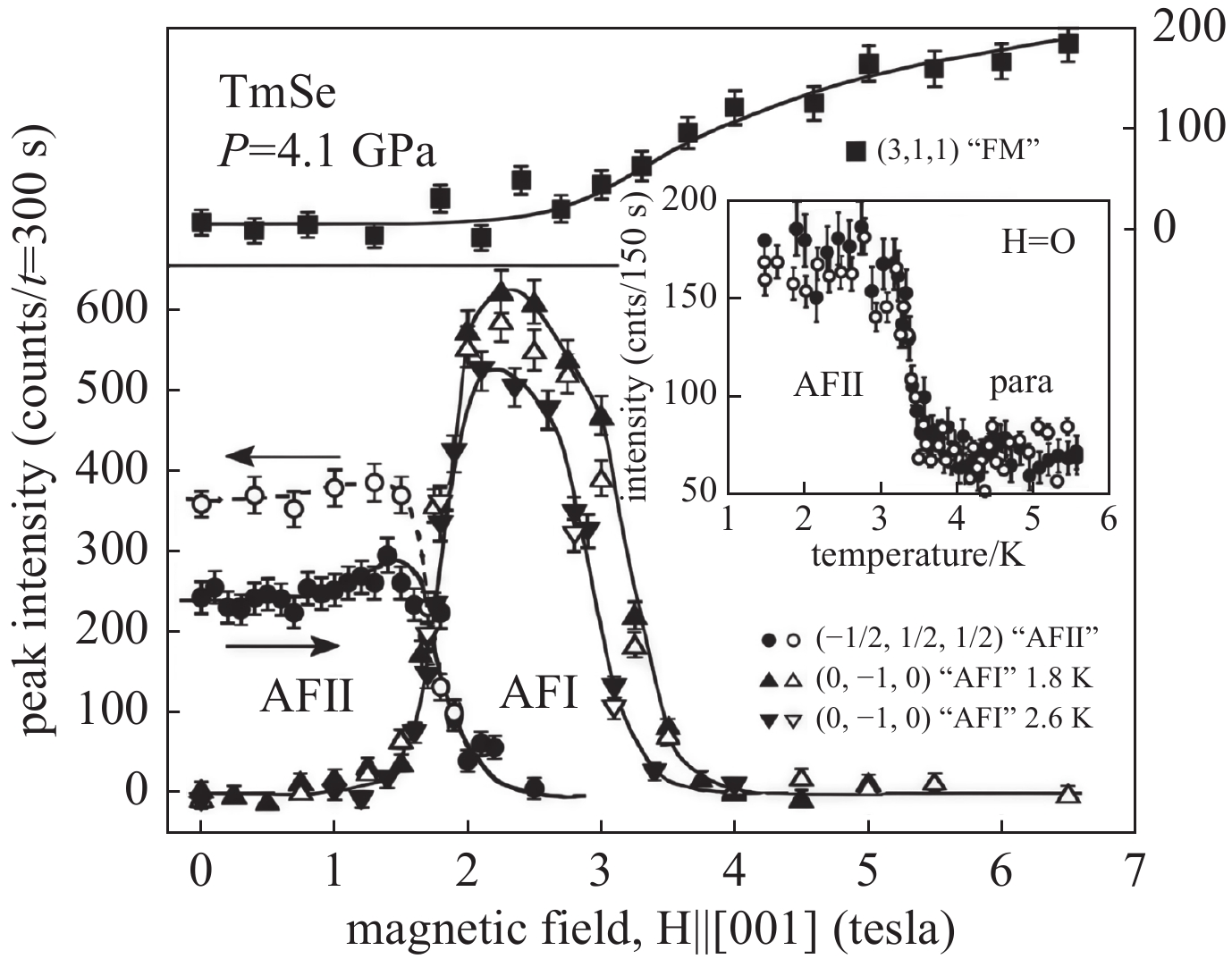
Mignot J M, Goncharenko I N, Matsumura T, et al. Magnetic phase diagram of the mixed-valence semiconductor TmSe under multi-extreme (P, H, T) conditions[J]. Physica B: Condensed Matter, 2005, 359/361: 105-107.
|
| [25] |
Giebultowicz T M, Rhyne J J, Furdyna J K, et al. Neutron diffraction study of the wurtzite-structure dilute magnetic semiconductor Zn0.45Mn0.55Se[J]. Journal of Applied Physics, 1987, 61(8): 3540-3542. doi: 10.1063/1.338717
|
| [26] |
熊振鹏. 宽禁带半导体GaN的辐照损伤机理研究[D]. 北京: 华北电力大学(北京), 2023
Xiong Zhenpeng. Research on radiation damage mechanism of wide band gap semiconductor GaN[D]. Beijing: North China Electric Power University (Beijing), 2023
|
| [27] |
周炜翔, 曹荣幸, 胡迪科, 等. 增强型Cascode结构GaN HEMT器件中子辐照效应研究[J]. 航天器环境工程, 2024, 41(5): 617-624 doi: 10.12126/see.2024010
Zhou Weixiang, Cao Rongxing, Hu Dike, et al. Study on neutron irradiation effects of enhancement-mode Cascode-structured GaN HEMT devices[J]. Spacecraft Environment Engineering, 2024, 41(5): 617-624 doi: 10.12126/see.2024010
|
| [28] |
Zhou Feng, Wang Tianqi, Liu Chaoming, et al. 800-V irradiation-hardened device technology on GaN-on-SiC power integration platform[C]//Proceedings of 2024 IEEE International Electron Devices Meeting. 2024.
|
| [29] |
Berthet F, Guhel Y, Boudart B, et al. Influence of thermal and fast neutron irradiation on dc electrical performances of AlGaN/GaN transistors[J]. IEEE Transactions on Nuclear Science, 2012, 59(5): 2556-2561. doi: 10.1109/TNS.2012.2209894
|
| [30] |
Brudnyi V N, Boiko V M, Kolin N G, et al. Neutron irradiation-induced modification of electrical and structural properties of GaN epifilms grown on Al2O3 (0001) substrate[J]. Semiconductor Science and Technology, 2018, 33: 095011. doi: 10.1088/1361-6641/aad53b
|
| [31] |
Butler P A, Uren M J, Lambert B, et al. Neutron irradiation impact on AlGaN/GaN HEMT switching transients[J]. IEEE Transactions on Nuclear Science, 2018, 65(12): 2862-2869. doi: 10.1109/TNS.2018.2880287
|
| [32] |
Gaubas E, Čeponis T, Meškauskaite D, et al. Pulsed photo-ionization spectroscopy of traps in as-grown and neutron irradiated ammonothermally synthesized GaN[J]. Scientific Reports, 2019, 9: 1473. doi: 10.1038/s41598-018-38138-6
|
| [33] |
Gaubas E, Vaitkus J, Kazlauskas K, et al. Recombination characteristics of the proton and neutron irradiated semi-insulating GaN structures[J]. Nuclear Instruments and Methods in Physics Research Section A: Accelerators, Spectrometers, Detectors and Associated Equipment, 2007, 583(1): 181-184.
|
| [34] |
谷文萍, 张林, 李清华, 等. 中子辐照对AlGaN/GaN 高电子迁移率晶体管器件电特性的影响[J]. 物理学报, 2014, 63: 047202 doi: 10.7498/aps.63.047202
Gu Wenping, Zhang Lin, Li Qinghua, et al. Effect of neutron irradiation on the electrical properties of AlGaN/GaN high electron mobility transistors[J]. Acta Physica Sinica, 2014, 63: 047202 doi: 10.7498/aps.63.047202
|
| [35] |
郝蕊静, 郭红霞, 潘霄宇, 等. AlGaN/GaN高电子迁移率晶体管器件中子位移损伤效应及机理[J]. 物理学报, 2020, 69: 207301 doi: 10.7498/aps.69.20200714
Hao Ruijing, Guo Hongxia, Pan Xiaoyu, et al. Neutron-induced displacement damage effect and mechanism of AlGaN/GaN high electron mobility transistor[J]. Acta Physica Sinica, 2020, 69: 207301 doi: 10.7498/aps.69.20200714
|
| [36] |
Kim B J, Kim H Y, Kim J, et al. Neutron irradiation on AlGaN/GaN high electron mobility transistors on SiC substrates[J]. Journal of Crystal Growth, 2011, 326(1): 205-207. doi: 10.1016/j.jcrysgro.2011.01.098
|
| [37] |
Rajan S, Waltereit P, Poblenz C, et al. Power performance of AlGaN–GaN HEMTs grown on SiC by plasma-assisted MBE[J]. IEEE Electron Device Letters, 2004, 25(5): 247-249. doi: 10.1109/LED.2004.826977
|
| [38] |
Kyle E C H, Kaun S W, Burke P G, et al. High-electron-mobility GaN grown on free-standing GaN templates by ammonia-based molecular beam epitaxy[J]. Journal of Applied Physics, 2014, 115: 193702. doi: 10.1063/1.4874735
|
| [39] |
Chen Jin, Puzyrev Y S, Zhang C X, et al. Proton-induced dehydrogenation of defects in AlGaN/GaN HEMTs[J]. IEEE Transactions on Nuclear Science, 2013, 60(6): 4080-4086. doi: 10.1109/TNS.2013.2281771
|
| [40] |
郝蕊静. GaN HEMT器件无偏置下中子位移损伤效应研究[D]. 湘潭: 湘潭大学, 2020
Hao Ruijing. The effect of neutron induced displacement damage in unbiased GaN HEMT devices[D]. Xiangtan: Xiangtan University, 2020
|
| [41] |
邱一武, 马艺珂, 张平威, 等. 增强型AlGaN/GaN HEMT器件中子位移损伤效应研究[J]. 固体电子学研究与进展, 2023, 43(4): 359-365,374
Qiu Yiwu, Ma Yike, Zhang Pingwei, et al. Study of neutron induced displacement damage in enhanced AlGaN/GaN HEMT device[J]. Research & Progress of SSE, 2023, 43(4): 359-365,374
|
| [42] |
Lorenz K, Marques J G, Franco N, et al. Defect studies on fast and thermal neutron irradiated GaN[J]. Nuclear Instruments and Methods in Physics Research Section B: Beam Interactions with Materials and Atoms, 2008, 266(12/13): 2780-2783.
|
| [43] |
Lv Ling, Li Peixian, Ma Xiaohua, et al. Fast and thermal neutron radiation effects on GaN PIN diodes[J]. IEEE Transactions on Nuclear Science, 2017, 64(1): 643-647. doi: 10.1109/TNS.2016.2630061
|
Figures(4)


 DownLoad: