

Research on efficient fabrication of nanogratings by space shaping femtosecond laser
-
摘要: 针对常规物镜聚焦飞秒激光光斑较小,难以单次直写加工成型大面积纳米光栅结构的问题,提出了利用空间狭缝整形的飞秒激光脉冲直写方法。通过开展单晶硅表面纳米光栅结构对加工系统的参数依赖关系研究,获得入射整形飞秒激光能量密度8.00 μJ/cm2、扫描速度9 mm/s、狭缝宽度0.40 mm的优化条件。采用SEM、AFM等手段对光栅进行微观表征,结果表明,单次扫描所制备的纳米光栅结构具有极高的宽度 (41.20 μm),说明提出的方法可以显著提升 一次成型大面积纳米光栅结构的制备效率。Abstract: Aiming at the difficulty of fabricating large-area nanograting structures with femtosecond laser in one step, the direct writing method of femtosecond laser pulse using slit-spatial shaping is proposed in this paper. By conducting a study on the parameter dependence of nanograting structures on the single-crystal silicon surface with the processing system, the optimized conditions of incident shaping femtosecond laser—energy density of 8.00 μJ/cm2, scanning speed of 9 mm/s, and slit width of 0.40 mm—are obtained. By using SEM, AFM and other microscopic characterization methods, it is indicated that the fabricated nanograting structure has an extremely high width (41.20 μm), greatly improving the fabrication efficiency of large-area nanograting structures in one step. This study provides a certain reference for the current research on efficiency optimizing and performance enhancing of femtosecond laser direct writing systems.
-
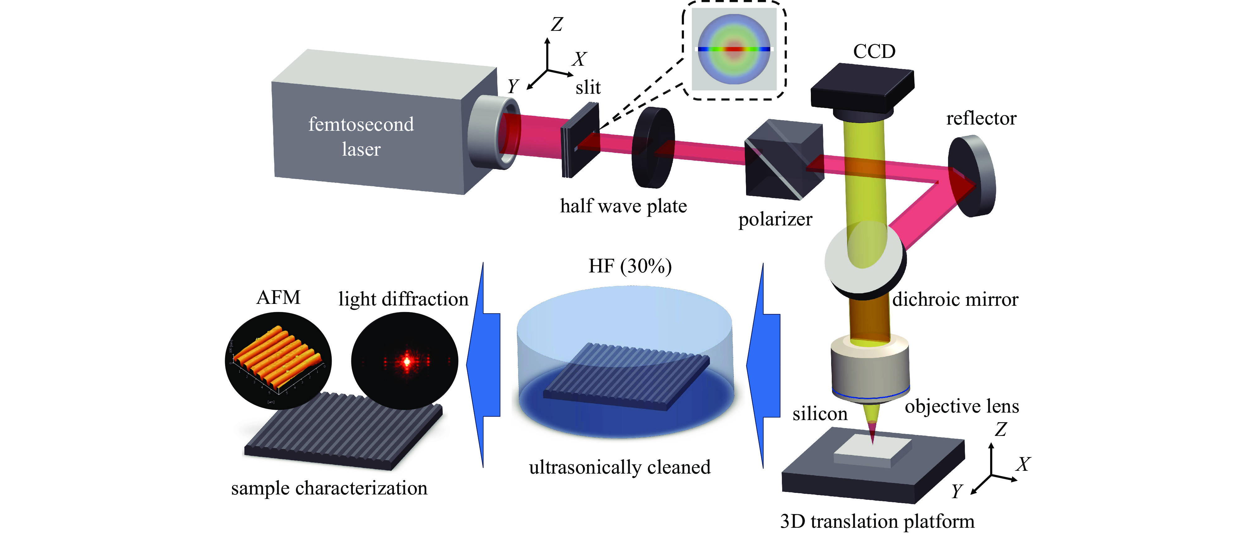
图 1 空间狭缝整形飞秒激光直写系统实验流程图
Figure 1. Experimental flowchart of spatial-shaped femtosecond laser direct writing
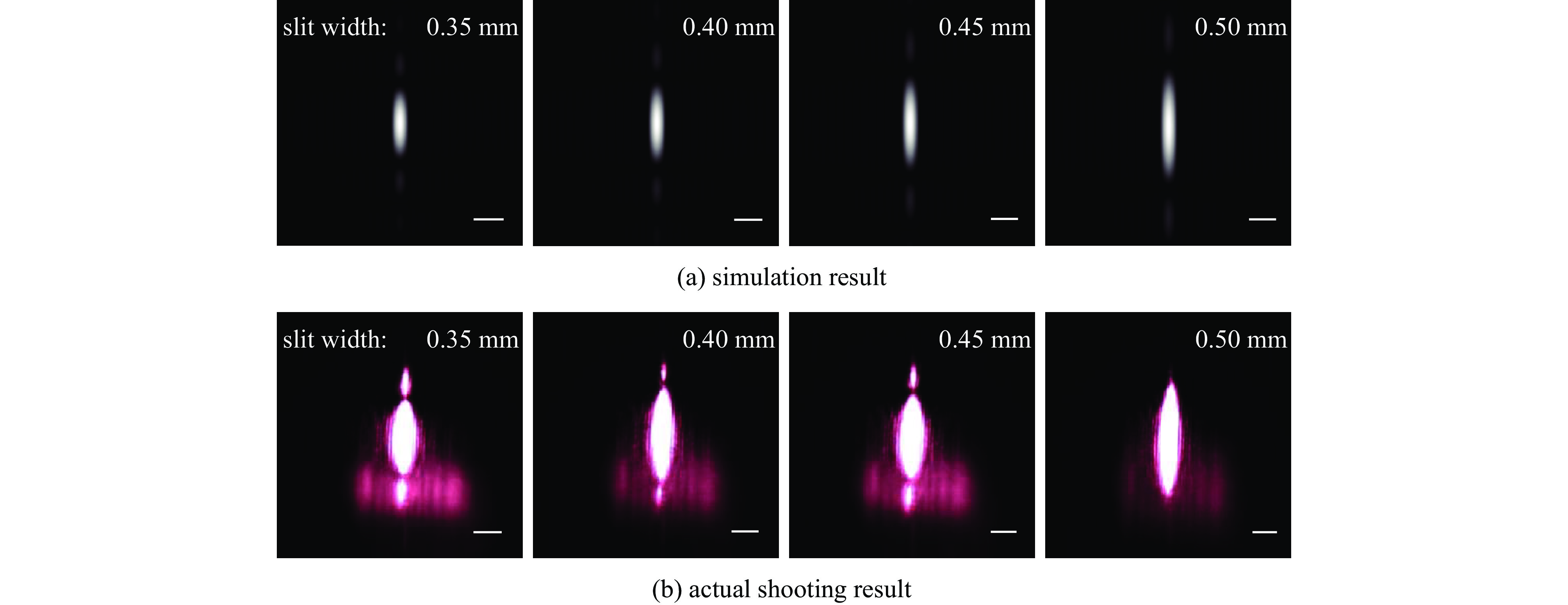
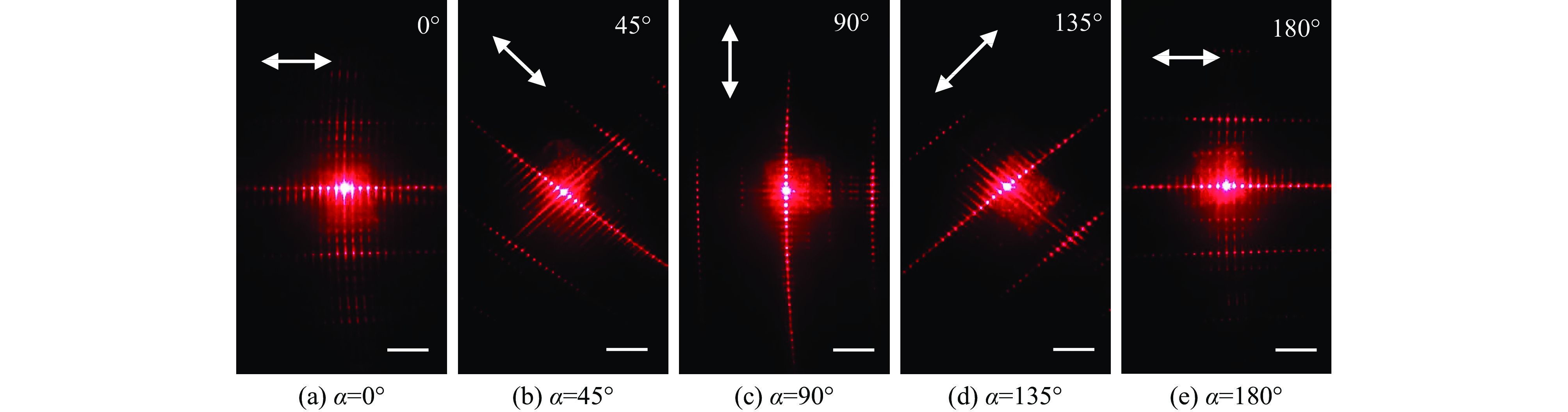
图 2 空间狭缝整形飞秒激光光斑衍射的仿真与实际拍摄结果,比例尺为10 μm
Figure 2. Simulation and actual shooting results of femtosecond laser spot diffraction through slit spatial shaping.The scale bar is 10 μm
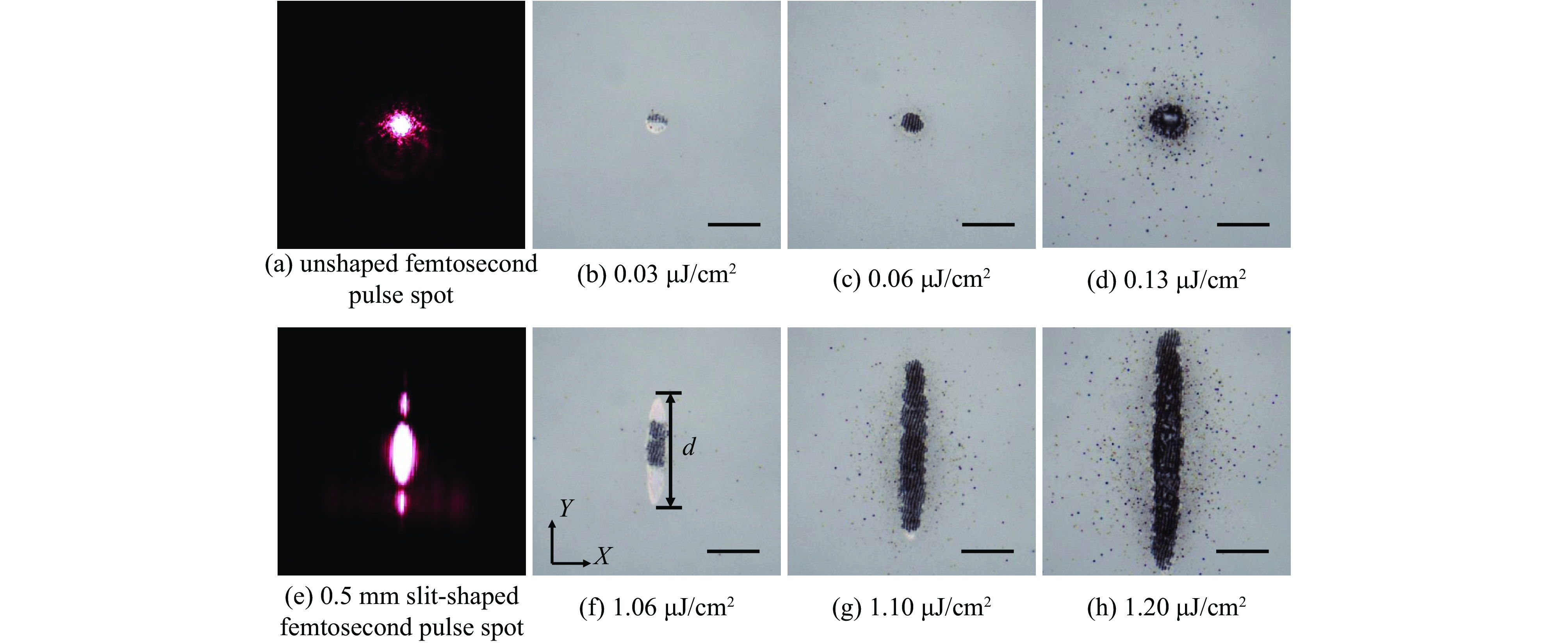
图 3 使用CCD拍摄的未整形fs脉冲光斑形貌和0.5 mm狭缝整形fs脉冲光斑形貌及其对应不同能量密度下加工结果。比例尺为5 μm
Figure 3. Unshaped fs pulse spot morphology and slit-shaped fs pulse spot morphology captured using CCD and their corresponding processing results at different energy densities. The scale bar is 5 μm
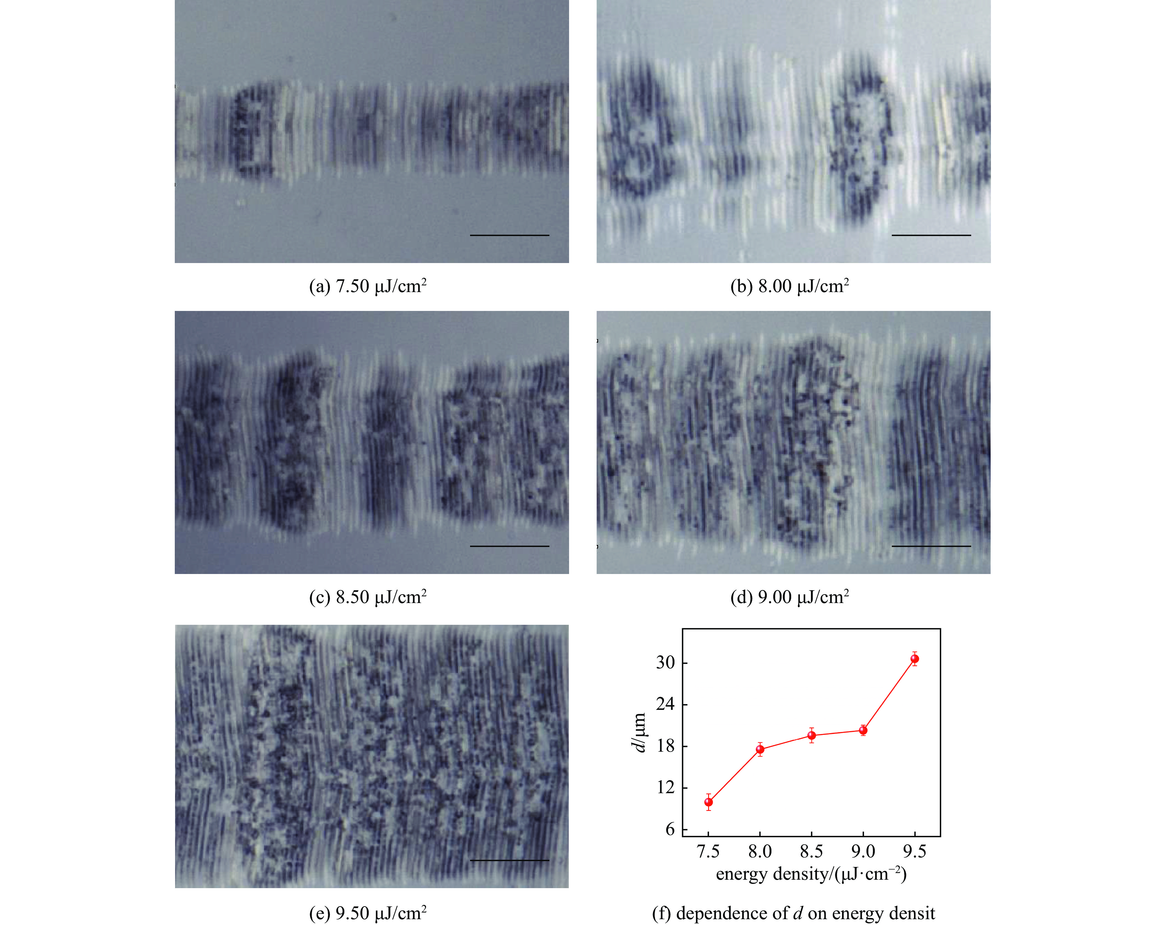
图 4 设置狭缝宽度为0.50 mm,扫描速度为9 mm/s,单晶硅表面纳米光栅在不同激光脉冲能量密度下的CCD图像。比例尺为10 μm
Figure 4. Setting the slit width at 0.50 mm and the scanning speed at 9 mm/s, CCD images of the nanograting structures on the surface of monocrystalline silicon at different laser pulse fluences are obtained. The scale bar is 10 μm

图 5 激光能量密度为8.50 μJ/cm2,狭缝宽度为0.50 mm,单晶硅表面纳米光栅在不同激光脉冲扫描速度下的CCD图像。比例尺为10 μm
Figure 5. Setting the laser energy density at 8.50 μJ/cm2 and the slit width at 0.50 mm, CCD images of the nanograting structures on the surface of monocrystalline silicon at different laser pulse scanning speeds are obtained. The scale bar is 10 μm
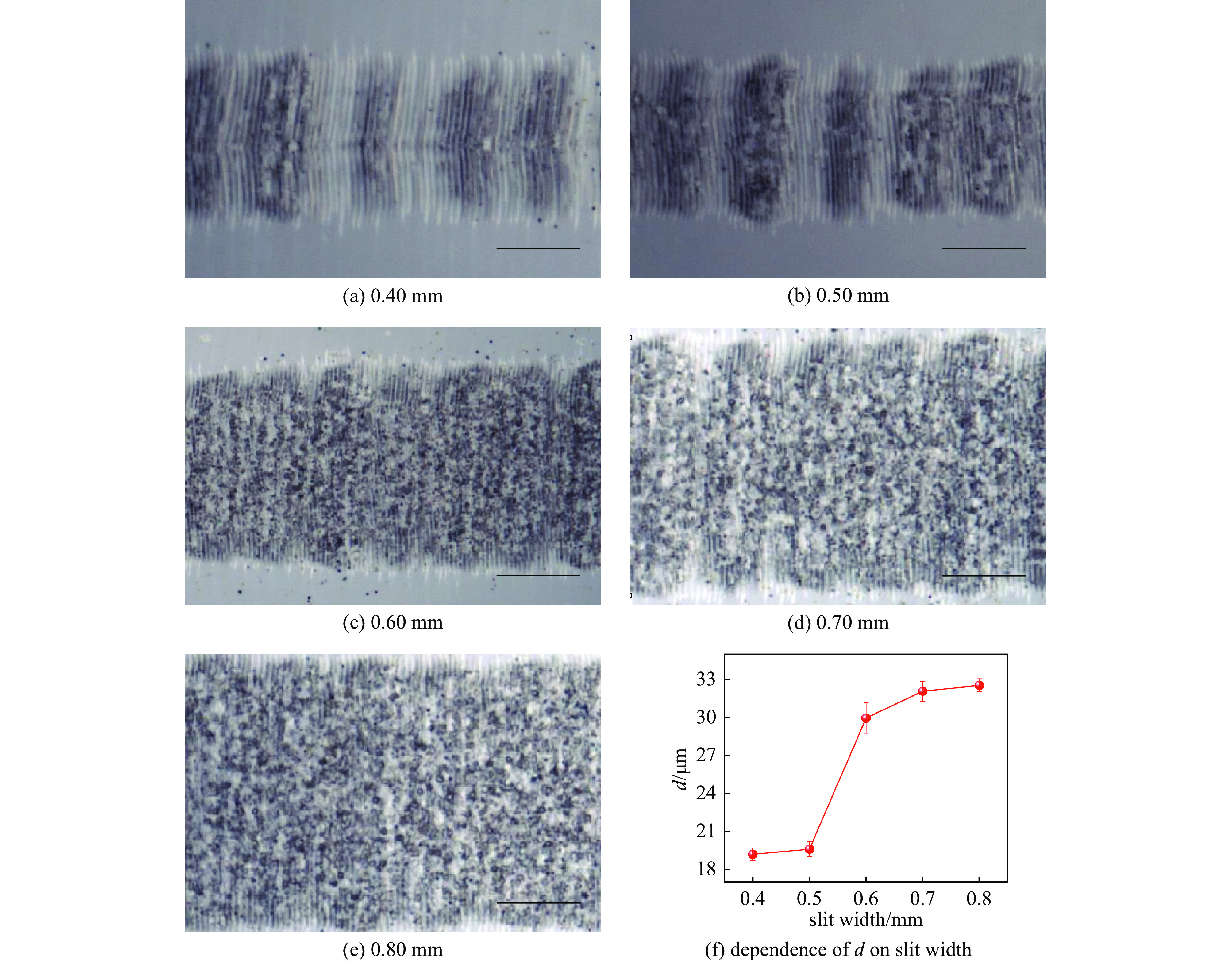
图 6 激光能量密度为8.50 μJ/cm2,扫描速度为9 mm/s,单晶硅表面纳米光栅在不同狭缝宽度下的CCD图像。比例尺为10 μm
Figure 6. Setting the laser energy density at 8.50 μJ/cm2 and the scanning speed at 9 mm/s, CCD images of the nanograting structures on the surface of monocrystalline silicon are captured at different slit widths. The scale is 10 μm
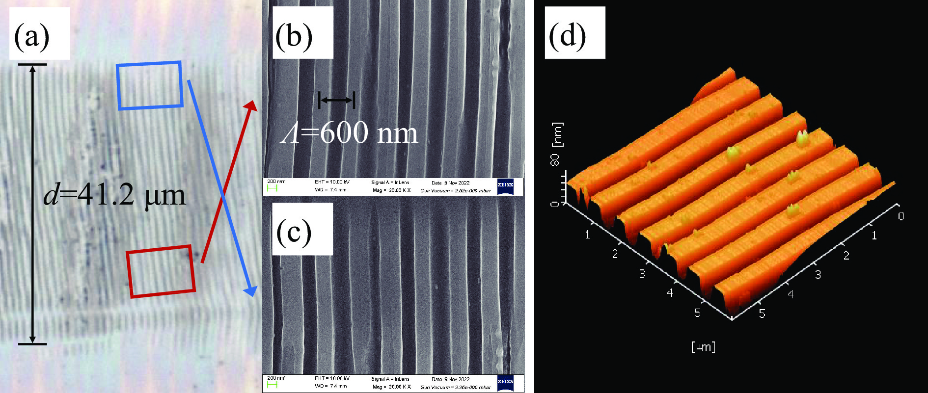
图 7 优化条件下制备的单晶硅表面纳米光栅结构
Figure 7. Nanograting structures on the surface of monocrystalline silicon fabricated under optimized conditions
-
[1] Xu Xiaoyi, Wang Tianxin, Chen Pengcheng, et al. Femtosecond laser writing of lithium niobate ferroelectric nanodomains[J]. Nature, 2022, 609(7927): 496-501. doi: 10.1038/s41586-022-05042-z [2] Pan Changji, Jiang Lan, Sun Jingya, et al. Ultrafast optical response and ablation mechanisms of molybdenum disulfide under intense femtosecond laser irradiation[J]. Light: Science & Applications, 2020, 9: 80. [3] Wu Meng, Xu Nianxi, Wang Erxi, et al. Nanogratings fabricated by wet etching assisted femtosecond laser modification of silicon for surface plasmon resonance sensing[J]. Applied Surface Science, 2022, 603: 154446. doi: 10.1016/j.apsusc.2022.154446 [4] Zhao Quanzhong, Qiu Jianrong, Zhao Chongjun, et al. Formation of arrayed holes on metal foil and metal film by multibeam interfering femtosecond laser beams[J]. Chinese Physics, 2005, 14(6): 1181-1184. doi: 10.1088/1009-1963/14/6/021 [5] 王锁成, 董世运, 闫世兴, 等. 飞秒激光制备金属表面微纳结构及其技术应用[J]. 激光与光电子学进展, 2023, 60:1700005Wang Suocheng, Dong Shiyun, Yan Shixing, et al. Fabrication of micro/nano structures on metal surfaces by femtosecond laser and its technical applications[J]. Laser & Optoelectronics Progress, 2023, 60: 1700005 [6] Oboňa J V, Skolski J Z P, Römer G R B E, et al. Pulse-analysis-pulse investigation of femtosecond laser-induced periodic surface structures on silicon in air[J]. Optics Express, 2014, 22(8): 9254-9261. doi: 10.1364/OE.22.009254 [7] 彭滟, 温雅, 张冬生, 等. 飞秒激光功率与脉冲数的比例关系对制备硅表面微结构的影响[J]. 中国激光, 2011, 38:1203005 doi: 10.3788/CJL201138.1203005Peng Yan, Wen Ya, Zhang Dongsheng, et al. Effect of the relation between femtosecond laser power and pulse number for fabricating surface-microstructured silicon[J]. Chinese Journal of Lasers, 2011, 38: 1203005 doi: 10.3788/CJL201138.1203005 [8] Liang Feng, Vallée R, Leang Chin S. Pulse fluence dependent nanograting inscription on the surface of fused silica[J]. Applied Physics Letters, 2012, 100: 251105. doi: 10.1063/1.4729620 [9] Li Yi, Liu Feng, Li Yanfeng, et al. Experimental study on GaP surface damage threshold induced by a high repetition rate femtosecond laser[J]. Applied Optics, 2011, 50(13): 1958-1962. doi: 10.1364/AO.50.001958 [10] Shen Mengyan, Carey J E, Crouch C H, et al. High-density regular arrays of nanometer-scale rods formed on silicon surfaces via femtosecond laser irradiation in water[J]. Nano Letters, 2008, 8(7): 2087-2091. doi: 10.1021/nl080291q [11] 王磊, 王熠, 王琳, 等. 飞秒激光直写偏振转换器件和几何相位器件(特邀)[J]. 光子学报, 2021, 50(6):38-49 doi: 10.3788/gzxb20215006.0650103Wang Lei, Wang Yi, Wang Lin, et al. Femtosecond laser direct writing for polarization convertors and geometric phase elements (Invited)[J]. Atca Photonica Sinica, 2021, 50(6): 38-49 doi: 10.3788/gzxb20215006.0650103 [12] Ulmeanu M, Jipa F, Radu C, et al. Large scale microstructuring on silicon surface in air and liquid by femtosecond laser pulses[J]. Applied Surface Science, 2012, 258(23): 9314-9317. doi: 10.1016/j.apsusc.2011.08.110 [13] Deng Guoliang, Feng Guoying, Liu Kui, et al. Temperature dependence of laser-induced micro/nanostructures for femtosecond laser irradiation of silicon[J]. Applied Optics, 2014, 53(14): 3004-3009. doi: 10.1364/AO.53.003004 [14] Feng Pin, Jiang Lan, Li Xin, et al. Gold-film coating assisted femtosecond laser fabrication of large-area, uniform periodic surface structures[J]. Applied Optics, 2015, 54(6): 1314-1319. doi: 10.1364/AO.54.001314 [15] 杨成娟, 梅雪松, 王文君, 等. 金铬薄膜的飞秒激光烧蚀加工[J]. 红外与激光工程, 2011, 40(1):61-65 doi: 10.3969/j.issn.1007-2276.2011.01.013Yang Chengjuan, Mei Xuesong, Wang Wenjun, et al. Femtosecond laser ablation on gold-chromium film[J]. Infrared and Laser Engineering, 2011, 40(1): 61-65 doi: 10.3969/j.issn.1007-2276.2011.01.013 [16] Pan An, Si Jinhai, Chen Tao, et al. Fabrication of two-dimensional periodic structures on silicon after scanning irradiation with femtosecond laser multi-beams[J]. Applied Surface Science, 2016, 368: 443-448. doi: 10.1016/j.apsusc.2016.01.269 [17] 王宇, 夏博, 万露露, 等. 飞秒激光辅助化学刻蚀透明材料微孔加工研究进展[J]. 激光与光电子学进展, 2022, 59:1900009Wang Yu, Xia Bo, Wan Lulu, et al. Study on femtosecond laser assisted chemical etching of transparent materials[J]. Laser & Optoelectronics Progress, 2022, 59: 1900009 [18] 袁春华, 李晓红, 唐多昌, 等. 不同气氛下飞秒激光诱导硅表面微结构[J]. 强激光与粒子束, 2010, 22(11):2749-2753 doi: 10.3788/HPLPB20102211.2749Yuan Chunhua, Li Xiaohong, Tang Duochang, et al. Silicon surface microstructures induced by femtosecond laser pulses in different background gases[J]. High Power Laser and Particle Beams, 2010, 22(11): 2749-2753 doi: 10.3788/HPLPB20102211.2749 [19] 李跃东, 尹唯一, 戴晔. 飞秒脉冲激光的时空变换影响纳米光栅直写过程的研究进展[J]. 激光与光电子学进展, 2020, 57:111403Li Yuedong, Yin Weiyi, Dai Ye. Research progress on spatio-temporal coupling of femtosecond pulse laser for direct-writing nanograting[J]. Laser & Optoelectronics Progress, 2020, 57: 111403 [20] Campillo A J, Pearson J E, Shapiro S L, et al. Fresnel diffraction effects in the design of high-power laser systems[J]. Applied Physics Letters, 1973, 23(2): 85-87. doi: 10.1063/1.1654817 [21] Wang Yuying, Zhong Lijing, Chen Zhi, et al. Photonic lattice-like waveguides in glass directly written by femtosecond laser for on-chip mode conversion[J]. Chinese Optics Letters, 2022, 20: 031406. doi: 10.3788/COL202220.031406 [22] 倪晓昌, 孙琦, 陈永耀, 等. 飞秒激光烧蚀材料表面产生纳米波纹结构的实验[J]. 纳米技术与精密工程, 2009, 7(1):47-50Ni Xiaochang, Sun Qi, Chen Yongyao, et al. Nano-ripples structure on material surface during femtosecond laser ablation[J]. Nanotechnology and Precision Engineering, 2009, 7(1): 47-50 -

 下载:
下载:
 点击查看大图
计量
- 文章访问数: 498
- HTML全文浏览量: 185
- PDF下载量: 69
- 被引次数: 0
