Research on the intensive model of PIN diode based on delayed breakdown characteristics
-
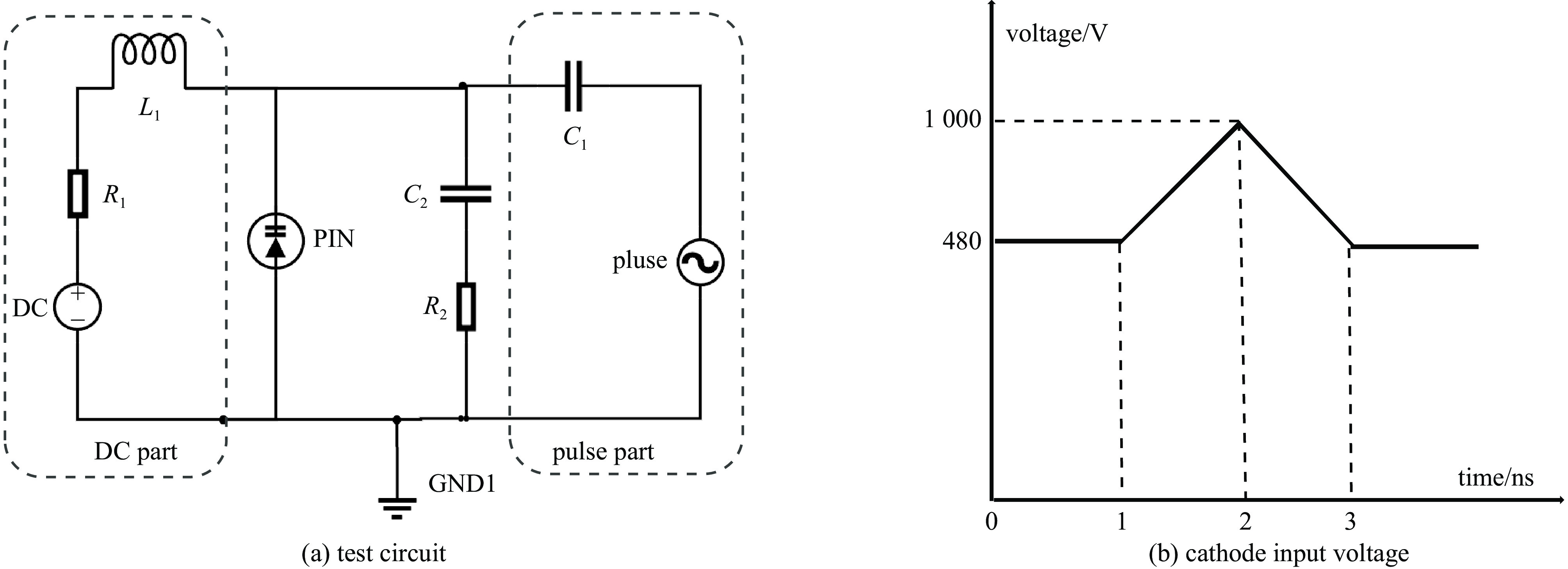
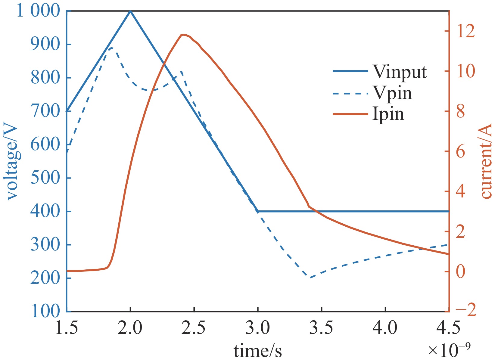
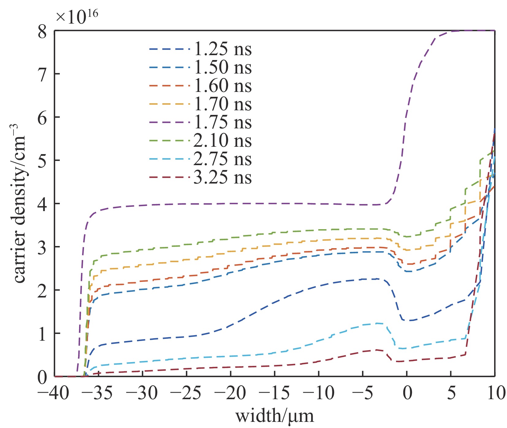
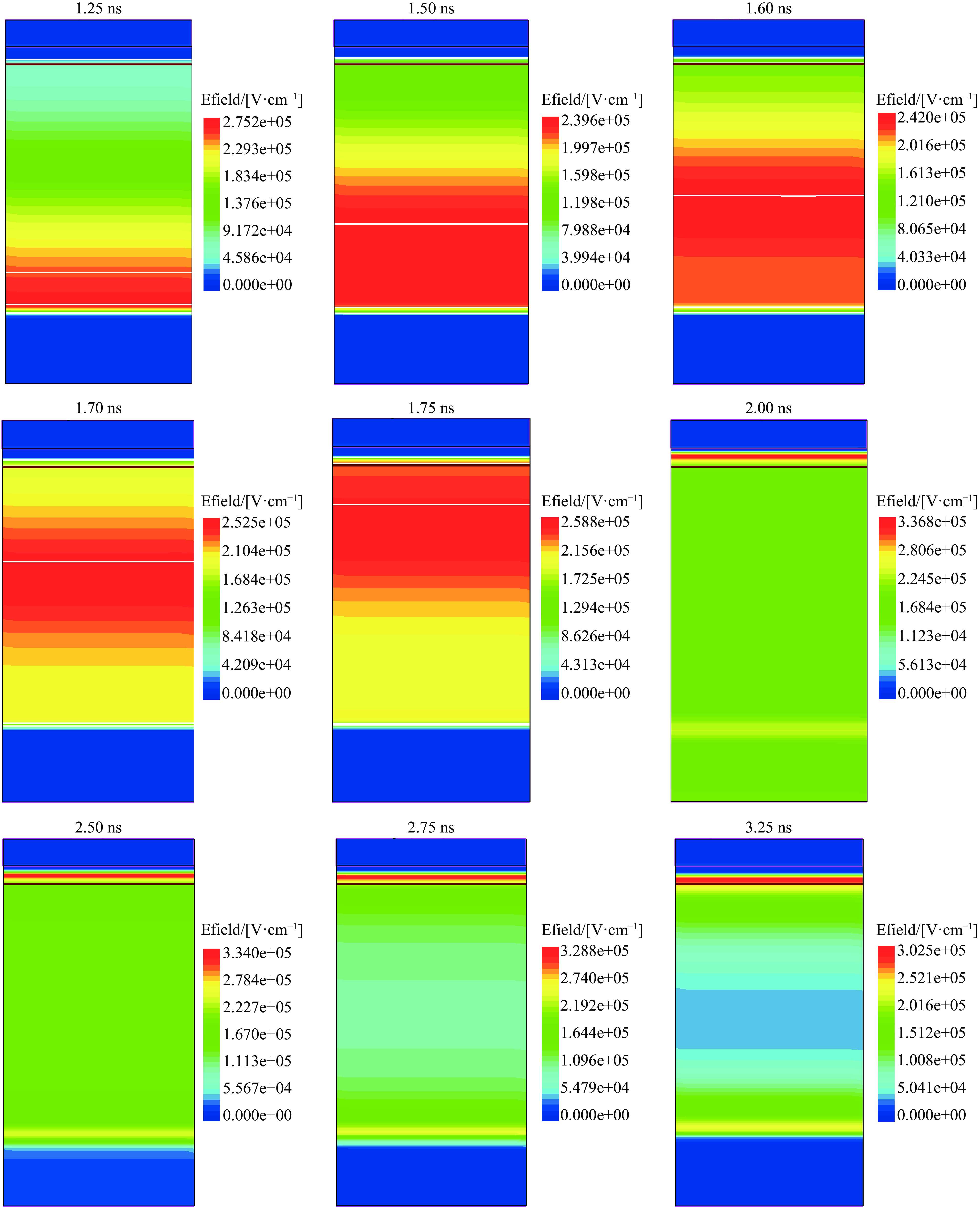
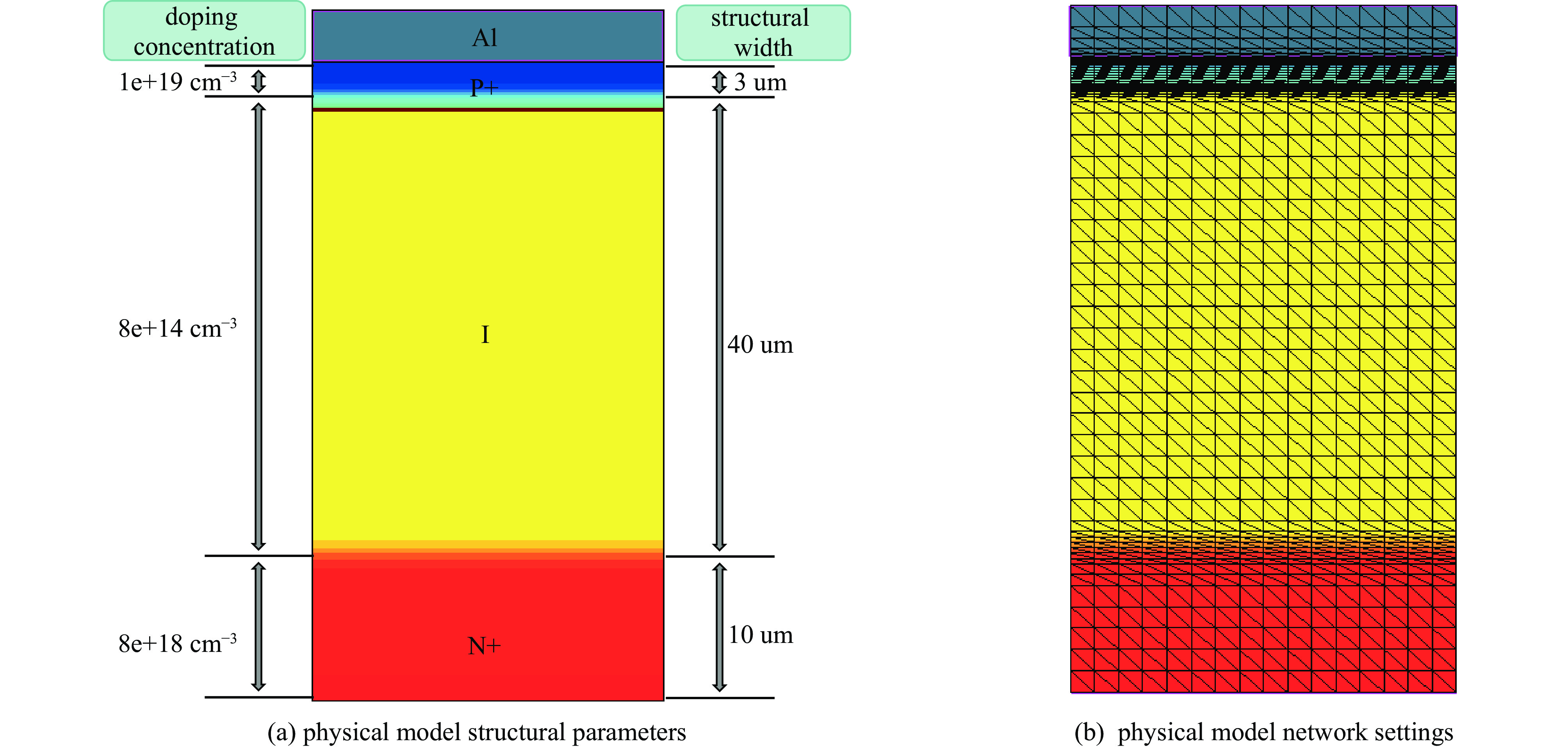
摘要: 延迟击穿特性在实现PIN二极管开关快速导通方面起着至关重要的作用。面对延迟击穿导通时间短导致物理过程分析困难的挑战,设计并验证了一种基于PIN结构的二极管集约模型。首先设计了一个基于PIN结构的二极管仿真模型,通过TCAD软件对该模型进行求解,结果显示在上升沿为520 V/ns、幅值为
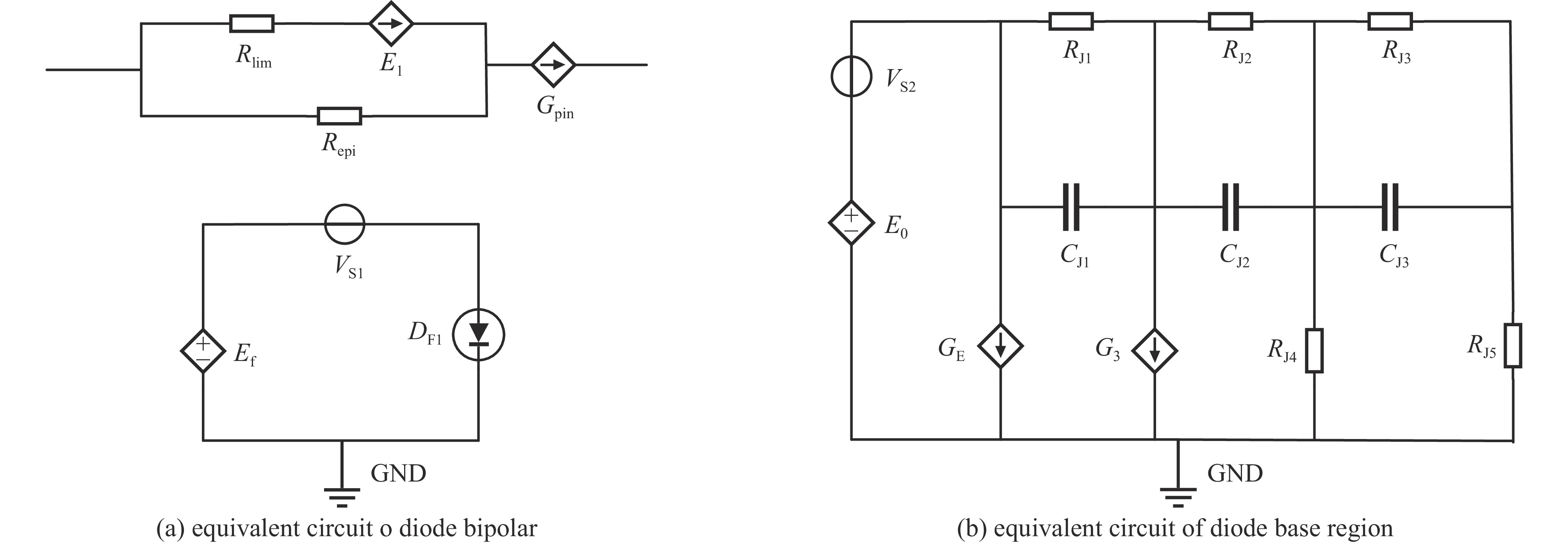
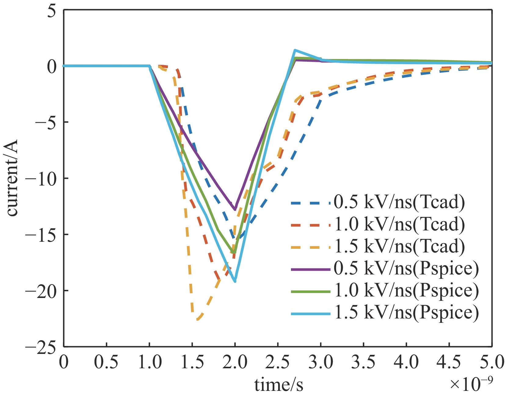
1000 V的快速高压触发脉冲作用下,二极管的击穿电压可达到其静态反向击穿电压的1.76倍,之后结合导通过程中的载流子浓度变化和电场变化情况对所建立模型的准确性作了进一步验证。其次,基于双极载流子扩散理论并结合TCAD仿真得到的参数,采用拉普拉斯变换和Pade逼近方法,对二极管的基区参数进行了等效电路处理。在此基础上利用基区的等效电路参数以及电导调制效应,建立了基于延迟击穿特性的PIN二极管集约模型。在Pspice软件中对该模型进行了仿真验证,结果显示在相同的触发脉冲作用下,二极管器件导通过程与TCAD仿真结果基本一致。本研究为探索快速导通二极管的反向延迟击穿特性提供了一种简单可行的电路分析方法。Abstract: The delayed breakdown characteristic is crucial for achieving the rapid conduction in PIN diodes. This paper addresses the challenges associated with analyzing the physical process involved in delayed breakdown conduction, primarily due to its short duration. An integrated diode model based on the PIN structure has been designed and validated in the study. Firstly, a numerical simulation model of the diode was developed using TCAD. The simulation results indicated that, influenced by a rapid rising high-voltage trigger pulse with a rise time of 520 V/ns and a magnitude of1000 V, the breakdown voltage of the diode could reach 1.76 times its static reverse breakdown voltage. The accuracy of the established model was further verified by examining changes in the carrier concentration and the evolution of the internal electric field during the conduction process. Secondly, based on bipolar carrier diffusion theory and the parameters obtained from TCAD simulations, the base region parameters of the diode were processed using the Laplace transform and Pade approximation method for equivalent circuit representation. Finally, utilizing the equivalent circuit parameters of the base region and considering conductance modulation effects, an integrated model of the PIN diode was constructed based on its delayed breakdown characteristics. This model was simulated and verified in Pspice software, demonstrating that under the same triggering pulse, the conduction process of the diode device is basically consistent with the TCAD simulation results. This study provides a straightforward and effective circuit analytic method for exploring the reverse delayed breakdown characteristics in rapidly conducting diodes.-
Key words:
- delayed breakdown /
- diode model /
- TCAD /
- bipolar carrier diffusion /
- Pspice
-
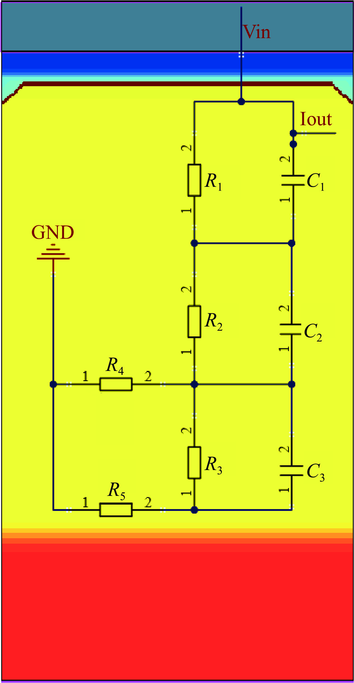
表 1 等效电路参数设置
Table 1. Equivalent circuit parameter settings
RJ1/Ω RJ2/Ω RJ3/Ω RJ4/Ω RJ5/Ω Rlim/mΩ Repi/Ω CJ1/µF CJ2/µF CJ3/µF 1 5 9 143 91 1.8 0.08 7.5 1.5 0.83 -
[1] 王欢, 乔汉青, 程骏, 等. 基极触发的雪崩晶体管导通机理[J]. 半导体技术, 2024, 49(5):432-441Wang Huan, Qiao Hanqing, Cheng Jun, et al. Conduction mechanism of base-triggered avalanche transistors[J]. Semiconductor Technology, 2024, 49(5): 432-441 [2] 马振宏, 刘振, 殷胜勇, 等. 高压纳秒脉冲电场消融黑色素瘤细胞实验研究[J]. 浙江大学学报(工学版), 2021, 55(6):1168-1174,1198 doi: 10.3785/j.issn.1008-973X.2021.06.018Ma Zhenhong, Liu Zhen, Yin Shengyong, et al. Experimental study on melanoma cell ablation by high-voltage nanosecond pulsed electric field[J]. Journal of Zhejiang University (Engineering Science), 2021, 55(6): 1168-1174,1198 doi: 10.3785/j.issn.1008-973X.2021.06.018 [3] 梁琳, 颜小雪, 黄鑫远, 等. 半导体脉冲功率开关器件综述[J]. 中国电机工程学报, 2022, 42(23):8631-8651Liang Lin, Yan Xiaoxue, Huang Xinyuan, et al. Review on semiconductor pulsed power switching devices[J]. Proceedings of the CSEE, 2022, 42(23): 8631-8651 [4] Mesyats G A, Yalandin M I. High-power picosecond electronics[J]. Physics-Uspekhi, 2005, 48(3): 211-229. doi: 10.1070/PU2005v048n03ABEH002113 [5] Grekhov I V, Kardo-Sysoev A F, Kostina L S, et al. High-power subnanosecond switch[J]. Electronics Letters, 1981, 17(12): 422-423. doi: 10.1049/el:19810293 [6] Grekhov I V, Kardo-Sysoev A F. Subnanosecond current drops in delayed breakdown of silicon p-n junctions[J]. Soviet Technical Physics Letters, 1979, 5(8): 395-396. [7] Ivanov M S, Podolska N I, Rodin P B. Quasi-streamer mode of delayed avalanche breakdown initiated by technological imperfections[J]. Journal of Physics: Conference Series, 2017, 816: 012033. doi: 10.1088/1742-6596/816/1/012033 [8] Rodin P B, Ivanov M. Spatiotemporal modes of fast avalanche switching of high-voltage layered semiconductor structures: from subnano to picosecond range[J]. Journal of Applied Physics, 2020, 127: 044504. doi: 10.1063/1.5097831 [9] Ivanov M, Brylevskiy V, Smirnova I, et al. Picosecond-range switching of high-voltage Si diode due to the delayed impact-ionization breakdown: experiments vs simulations[J]. Journal of Applied Physics, 2022, 131: 014502. doi: 10.1063/5.0077092 [10] Peng Xin, Liu Yong, Feng Hao, et al. Analysis and characterization of the Punchthrough n-p-n diode for hard switching power control applications[J]. IEEE Transactions on Electron Devices, 2023, 70(9): 4525-4531. doi: 10.1109/TED.2023.3294358 [11] Zhang Manhong. A modified finite difference model to the reverse recovery of silicon PIN diodes[J]. Solid-State Electronics, 2020, 171: 107839. doi: 10.1016/j.sse.2020.107839 [12] Brylevskiy V, Podolska N, Smirnova I, et al. Picosecond-range avalanche switching initiated by a steep high-voltage pulse: Si bulk samples versus layered pn junction structures[J]. Physica Status Solidi (b), 2019, 256: 1800520. doi: 10.1002/pssb.201800520 [13] Okuto Y, Crowell C R. Threshold energy effect on avalanche breakdown voltage in semiconductor junctions[J]. Solid-State Electronics, 1975, 18(2): 161-168. doi: 10.1016/0038-1101(75)90099-4 [14] Potbhare S, Goldsman N, Lelis A, et al. A physical model of high temperature 4H-SiC MOSFETs[J]. IEEE Transactions on Electron Devices, 2008, 55(8): 2029-2040. doi: 10.1109/TED.2008.926665 [15] Brylevskiy V I, Smirnova I A, Podolska N I, et al. Experimental observation of delayed impact-ionization avalanche breakdown in semiconductor structures without p-n junctions[J]. Technical Physics Letters, 2018, 44(2): 160-163. doi: 10.1134/S1063785018020177 [16] 黄鑫远. 快速离化晶体管优化设计和失效分析研究[D]. 武汉: 华中科技大学, 2022: 67-68Huang Xinyuan. Study on optimal design and failure analysis of fast ionization dynistor[D]. Wuhan: Huazhong University of Science and Technology, 2022: 67-68 [17] 周瑜. 4H-SiC等离子体波开关器件研究[D]. 西安: 西安电子科技大学, 2022: 37-39Zhou Yu. Research on 4H-SiC plasma wave switching devices[D]. Xi'an: Xidian University, 2022: 37-39 [18] 张佳佳, 叶尚斌, 张逸成, 等. 基于拉氏变换的变温度PIN二极管动态建模[J]. 电工技术学报, 2016, 31(1):139-146 doi: 10.3969/j.issn.1000-6753.2016.01.017Zhang Jiajia, Ye Shangbin, Zhang Yicheng, et al. Temperature-variable dynamic modeling of PIN diode based on Laplace transform[J]. Transactions of China Electrotechnical Society, 2016, 31(1): 139-146 doi: 10.3969/j.issn.1000-6753.2016.01.017 [19] 盛定仪, 杨耿, 谭吉春, 等. 功率PIN二极管PSpice子电路模型[J]. 现代电子技术, 2008(6):141-143 doi: 10.3969/j.issn.1004-373X.2008.06.049Sheng Dingyi, Yang Geng, Tan Jichun, et al. A new power PIN diode PSpice subcircuit Model[J]. Modern Electronics Technique, 2008(6): 141-143 doi: 10.3969/j.issn.1004-373X.2008.06.049 [20] 李鑫, 罗毅飞, 段耀强, 等. 一种基于集总电荷的大功率PIN二极管改进电路模型[J]. 电工技术学报, 2019, 34(3):506-515Li Xin, Luo Yifei, Duan Yaoqiang, et al. An improved lumped-charge circuit model for high power PIN diode[J]. Transactions of China Electrotechnical Society, 2019, 34(3): 506-515 -


 下载:
下载:
