

Total ionizing dose effect on gate drivers fabricated by BCD technology
-
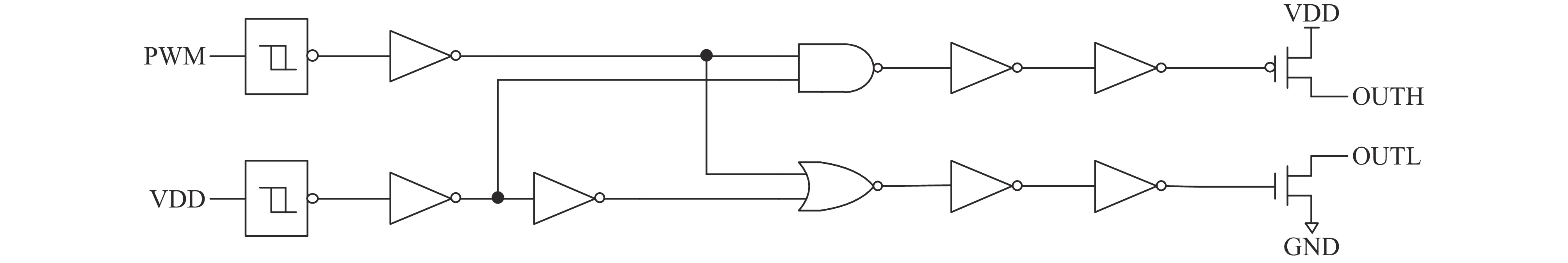
摘要: 针对一款BCD工艺栅极驱动器,采用环栅结构进行总剂量效应加固。通过60Co γ辐照试验,对比了加固和非加固器件电学参数随剂量变化情况。结果表明,总剂量辐射会导致器件的输出电压与电流特性发生退化,出现转换电压下降与输出电流上升的现象,同时发现总剂量辐射对输出电阻几乎无影响。对比两种栅极驱动器辐照前后的测试结果,证明环栅加固方法对抑制总剂量辐射引起的边缘漏电有一定的效果,但辐照总剂量达到500 krad(Si)时,加固器件发生功能失效。通过仿真模拟各级晶体管辐射损伤对器件最终输出结果的影响,确定初级施密特反相器内阈值电压漂移影响转换电压,而末级晶体管阈值电压漂移导致输出高电平下降。Abstract: The BCD technology integrates Bipolar, Complementary Metal Oxide Semiconductor (CMOS), and Double Diffused MOSFET (DMOS) within a single chip, widely utilized in electronic components and system production. Gate drivers fabricated by BCD technology can reduce transmission delays, lower power consumption, and enhance drive capabilities. However, the radiation effects in space environments may lead to performance degradation and potentially jeopardize the safety of spacecraft. This paper focuses on gate drivers based on BCD technology, employing an enclosed layout structure for total ionizing dose (TID) radiation hardening. Through TID irradiation tests, the electrical parameter variations between hardened and unhardened devices are compared. Results indicate that TID radiation causes degradation in the output voltage and current characteristics of the device, manifesting as a decrease in switching voltage and an increase in output current, while having a negligible impact on the output resistance. Comparing test outcomes from both types of drivers, it is evident that the ring-gate hardening method effectively mitigates edge leakage induced by TID radiation to a certain extent. Nevertheless, functional failure occurs in the devices at 500 krad(Si).
-
Key words:
- BCD technology /
- gate driver /
- total ionizing dose effect /
- enclosed layout device
-
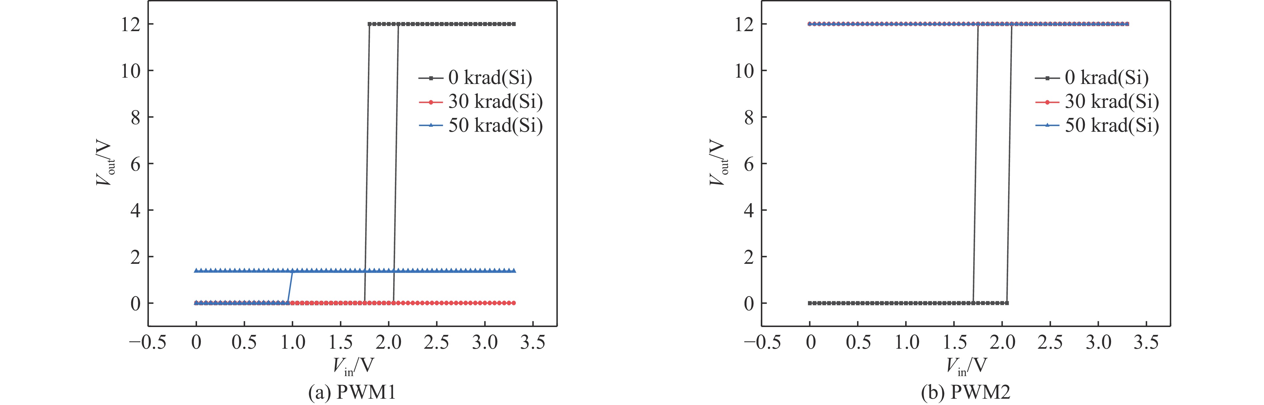
图 2 非加固器件输出电压随辐照剂量的变化
Figure 2. Variation of output voltage of unhardened devices with irradiation dose
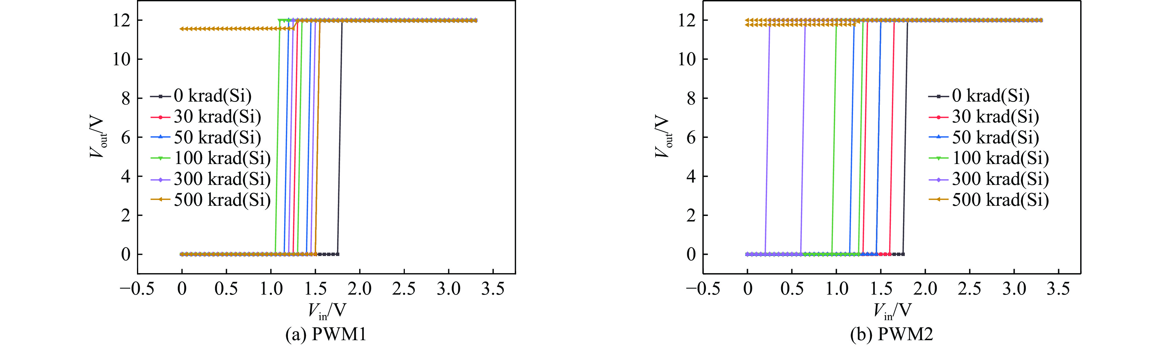
图 3 加固器件输出电压随辐照剂量的变化
Figure 3. Variation of output voltage of hardened devices with irradiation dose
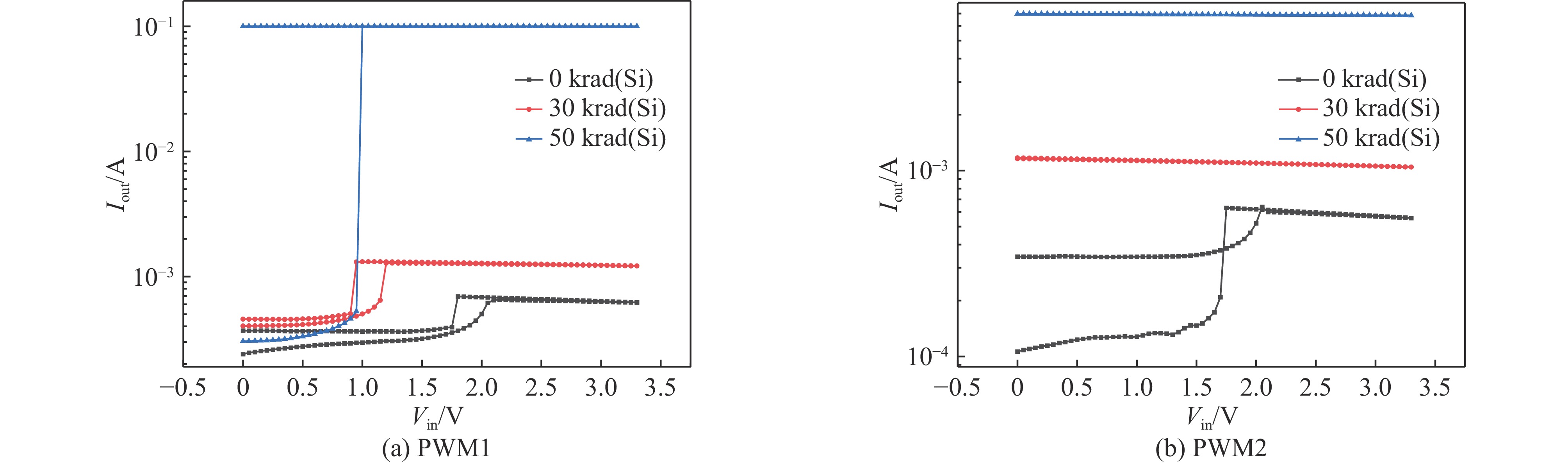
图 4 非加固器件输出电流随辐照剂量的变化
Figure 4. Variation of output current of unhardened devices with irradiation dose
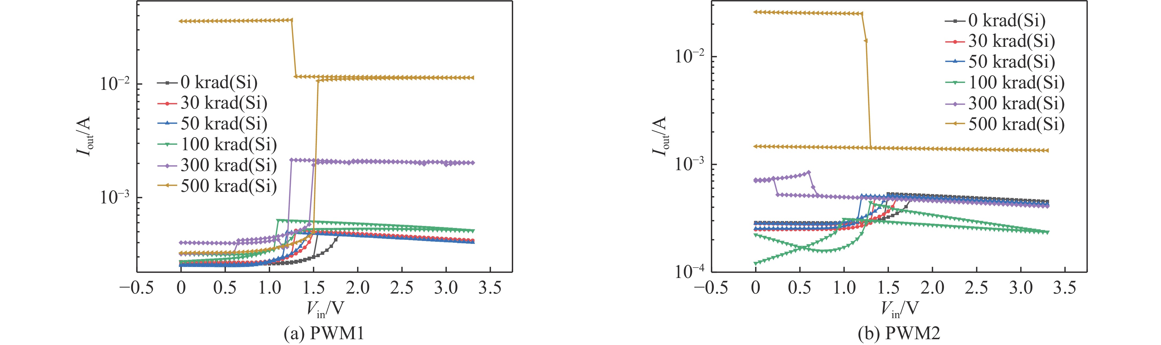
图 5 加固器件输出电流随辐照剂量的变化
Figure 5. Variation of output current of hardened devices with irradiation dose
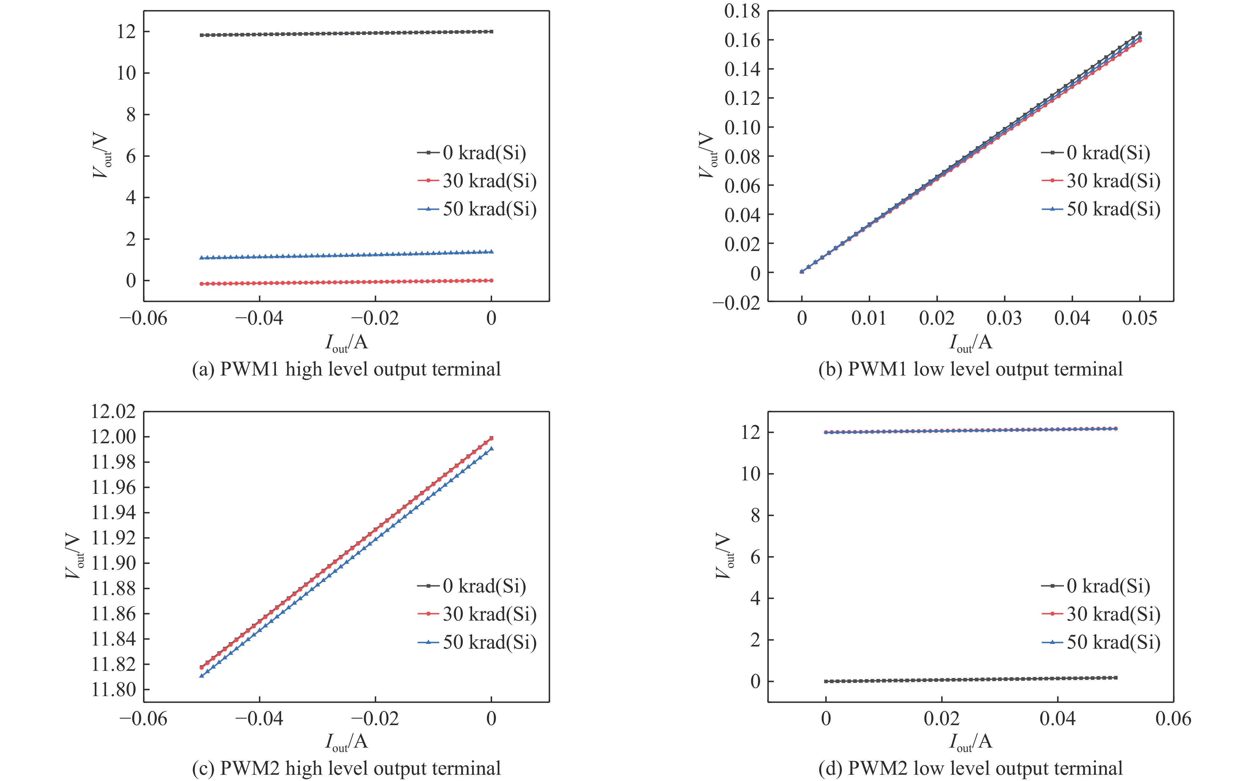
图 6 非加固器件各端口输出电阻随辐照剂量变化情况
Figure 6. Variation of output resistance of unhardened devices with irradiation dose
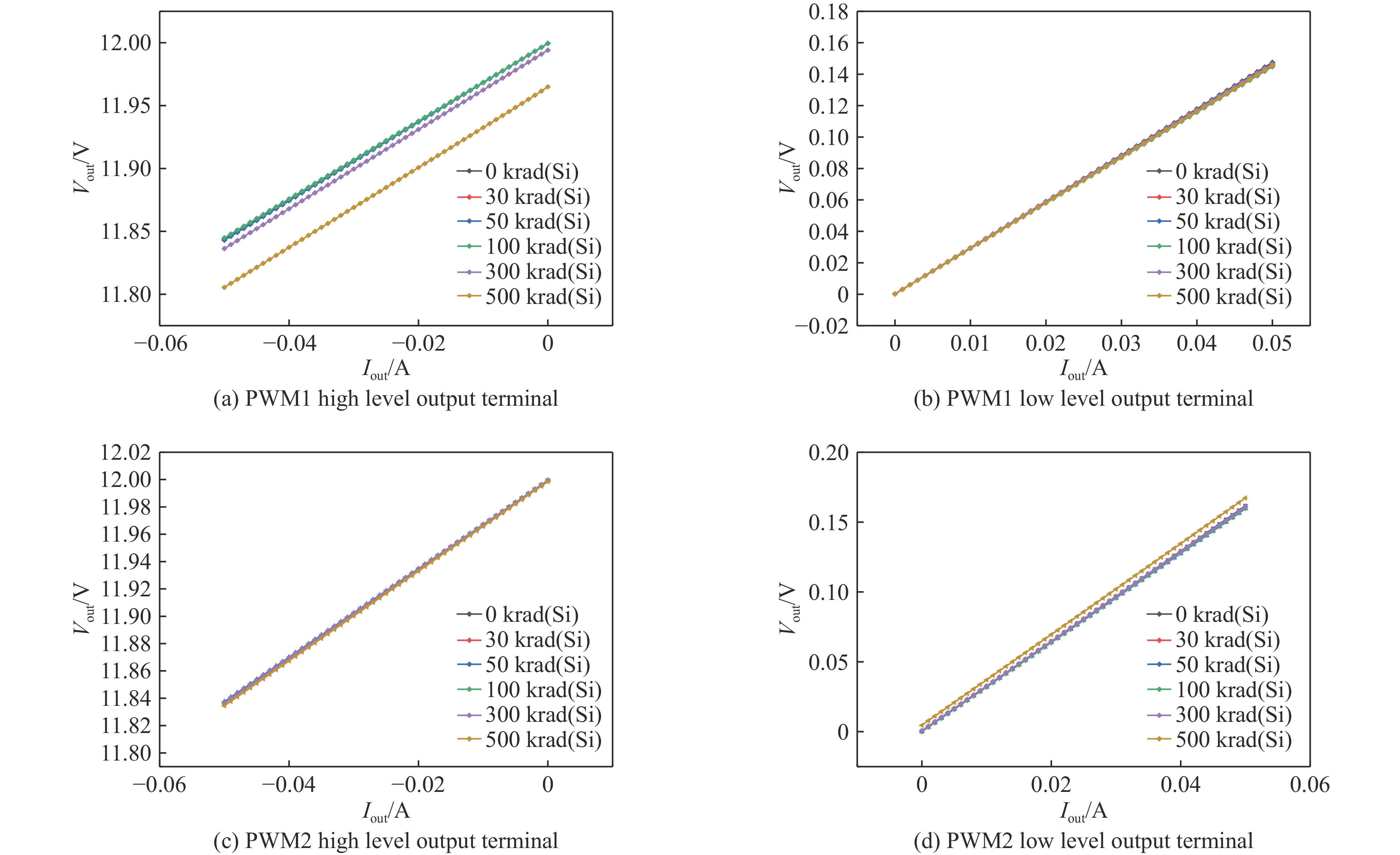
图 7 加固器件各端口输出电阻随辐照剂量变化情况
Figure 7. Variation of output resistance of hardened devices with irradiation dose
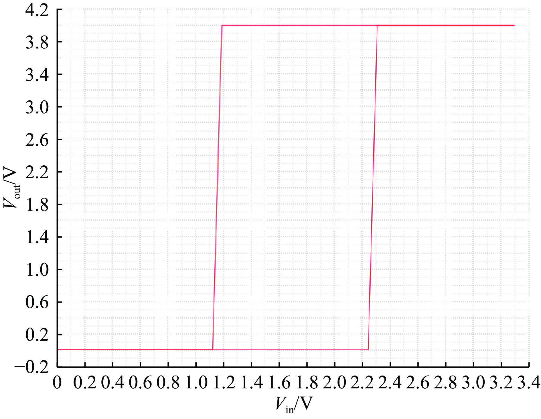
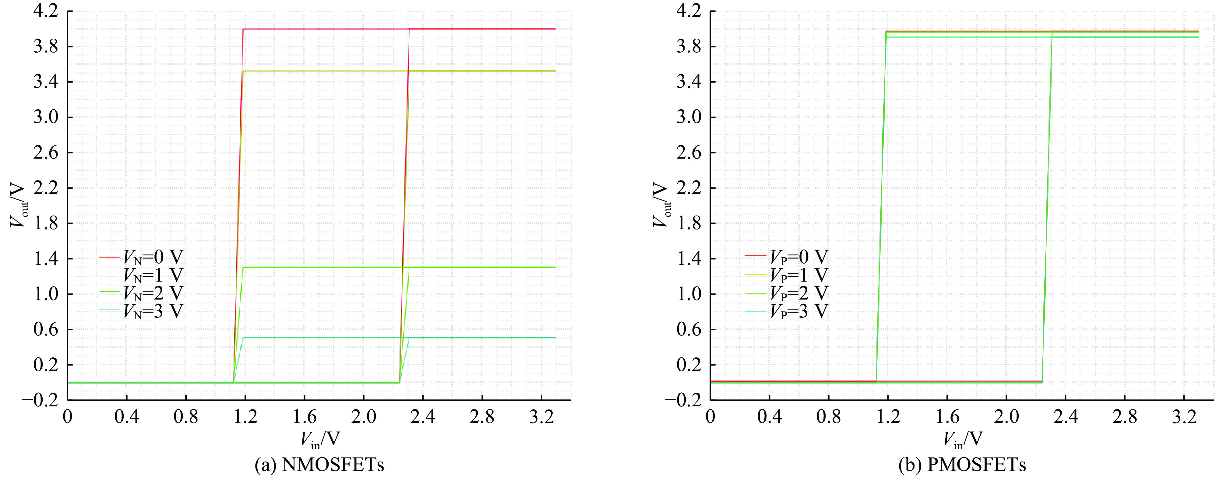
图 9 仿真电路输出电压随输入电压的变化曲线
Figure 9. Simulation curve of output voltage varying with input voltage in the circuit
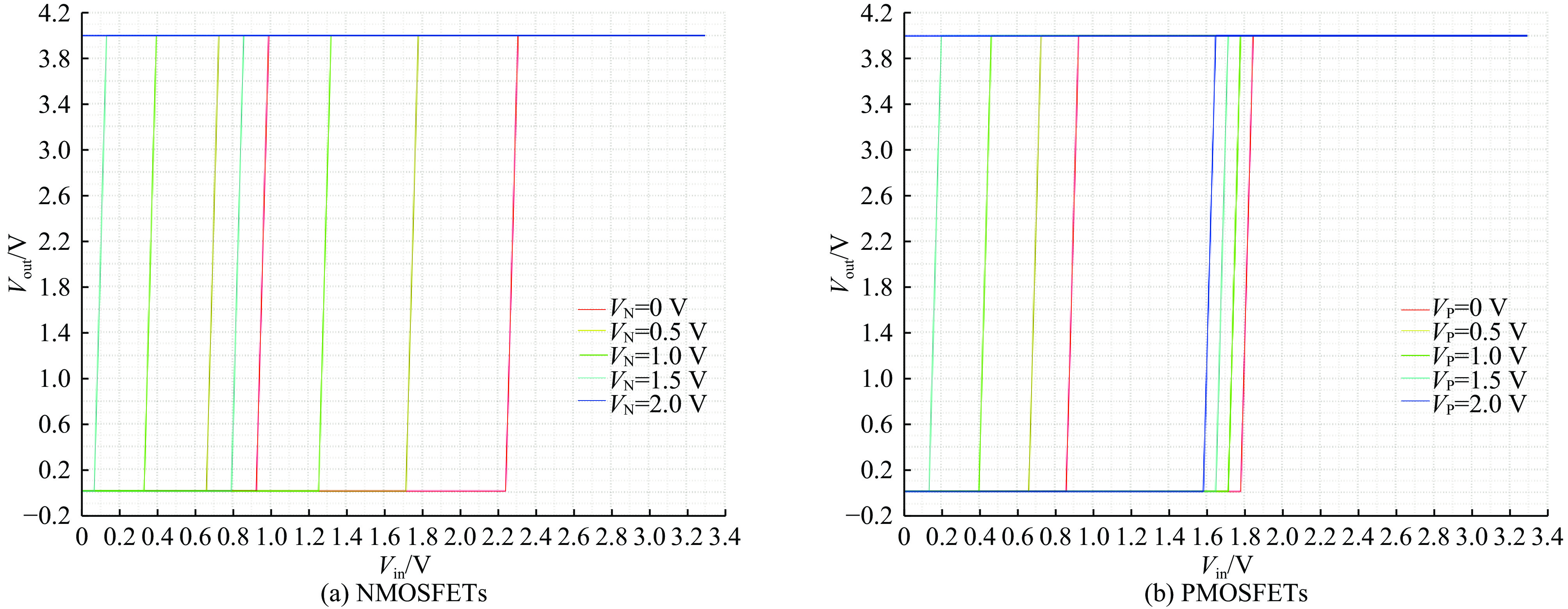
图 10 仿真电路输出电压曲线随施密特反相器内器件阈值电压漂移程度的变化
Figure 10. Simulation curves of output voltage variation with threshold voltage shift in MOSFETs within the Schmitt trigger inverter
-
[1] 张为, 陈曙光. 一种新型的BCD工艺栅驱动集成电路[J]. 北京理工大学学报, 2011, 31(9):1080-1084Zhang Wei, Chen Shuguang. A novel gate driver IC based on BCD technology[J]. Transactions of Beijing Institute of Technology, 2011, 31(9): 1080-1084 [2] 吴琼乐. 一种基于BCD工艺的高压栅驱动电路设计[D]. 成都: 电子科技大学, 2012Wu Qiongle. Design of a high-voltage gate driver circuit based on BCD process[D]. Chengdu: University of Electronic Science and Technology of China, 2012 [3] 周锌, 陈浪涛, 乔明, 等. 抗辐射高压集成电路技术现状与发展[J]. 微电子学与计算机, 2022, 39(10):1-16 doi: 10.3969/j.issn.1000-7180.2022.10.wdzxyjsj202210001Zhou Xin, Chen Langtao, Qiao Ming, et al. The development of radiation-hardened high voltage integrated circuits[J]. Microelectronics & Computer, 2022, 39(10): 1-16 doi: 10.3969/j.issn.1000-7180.2022.10.wdzxyjsj202210001 [4] 孙伟锋, 张波, 肖胜安, 等. 功率半导体器件与功率集成技术的发展现状及展望[J]. 中国科学: 信息科学, 2012, 42(12):1616-1630 doi: 10.1360/112012-510Sun Weifeng, Zhang Bo, Xiao Sheng’an, et al. Development and trend of power semiconductor devices and power integrated technology[J]. Scientia Sinica (Informationis), 2012, 42(12): 1616-1630 doi: 10.1360/112012-510 [5] Zhang Zhengyuan, Feng Zhicheng, Li Xiaogang, et al. A research for BCD compatible technology[C]//Proceedings of 2008 9th International Conference on Solid-State and Integrated-Circuit Technology. Beijing, 2008: 192-194. [6] Ma Xiaobo, Thant Z T, Jiang Huihua, et al. Integration of split-gate flash memory in 130 nm BCD technology for automotive applications[C]//Proceedings of 2019 Electron Devices Technology and Manufacturing Conference (EDTM). 2019: 318-320. [7] Antonov A A, Karpovich M S, Vasilyev V Y. Dual 4-a high-speed low-side gate driver IC for GaN and Si MOSFETs and IGBTs[C]//Proceedings of 2022 IEEE 23rd International Conference of Young Professionals in Electron Devices and Materials (EDM). 2022: 378-382. [8] Cao Jianwen, Zhou Zekun, Shi Yue, et al. An integrated gate driver based on SiC MOSFETs adaptive multi-level control technique[J]. IEEE Transactions on Circuits and Systems I: Regular Papers, 2023, 70(4): 1805-1816. doi: 10.1109/TCSI.2023.3233956 [9] Park I Y, Choi Y K, Ko K Y, et al. BCD (Bipolar-CMOS-DMOS) technology trends for power management IC[C]//Proceedings of the 8th International Conference on Power Electronics - ECCE Asia. 2011: 318-325. [10] 凌荣勋. 抗辐射功率集成电路的关键技术研究及实现[D]. 成都: 电子科技大学, 2020Ling Rongxun. Research and implementation of key technologies for radiation-hard power integrated circuits[D]. Chengdu: University of Electronic Science and Technology of China, 2020 [11] Zhou Xiao, Luo Ping, He Linyan, et al. A radiation-hard waffle layout for BCD power MOSFET[C]//Proceedings of 2017 IEEE 12th International Conference on ASIC (ASICON). 2017: 773-775. [12] 赵双龙. BCD工艺在电源管理IC设计中的应用[D]. 杭州: 浙江大学, 2006Zhao Shuanglong. Application of BCD process in power management IC design[D]. Hangzhou: Zhejiang University, 2006 [13] 王鹏, 徐青, 杭丽, 等. 一种抗辐射高压MOSFET驱动器的设计[J]. 太赫兹科学与电子信息学报, 2016, 14(6):972-976 doi: 10.11805/TKYDA201606.0972Wang Peng, Xu Qing, Hang Li, et al. A design of radiation hardening high-voltage MOSFET driver[J]. Journal of Terahertz Science and Electronic Information Technology, 2016, 14(6): 972-976 doi: 10.11805/TKYDA201606.0972 [14] 冯垚荣. 一种抗辐照栅驱动电路设计[D]. 成都: 电子科技大学, 2019Feng Yaorong. The design of a radiation-hardened gate drive circuit[D]. Chengdu: University of Electronic Science and Technology of China, 2019 [15] 关晓明. 抗辐照高压栅驱动电路的设计[D]. 成都: 电子科技大学, 2020Guan Xiaoming. Design of radiation-hard high-voltage gate driver circuit[D]. Chengdu: University of Electronic Science and Technology of China, 2020 [16] Lai Rongxing, Fang Jian, Guan Xiaoming, et al. A radiation-hard gate driver circuit for high voltage application[C]//Proceedings of 2020 32nd International Symposium on Power Semiconductor Devices and ICs (ISPSD). 2020: 262-265. [17] Lei Xin, Gao Xingguo, Deng Jun, et al. A 15-V tolerant and radiation-hardened MOSFET driver with positive and negative references[J]. IEEE Transactions on Aerospace and Electronic Systems, 2023, 59(2): 851-857. [18] Lu Yu, Cai Xiaowu, Dang Jianying, et al. A novel radiation-hardened level shifter with dV/dt noise immunity for 600-V HVIC[J]. IEEE Transactions on Nuclear Science, 2024, 71(9): 2086-2093. doi: 10.1109/TNS.2024.3434338 [19] Schwank J R, Shaneyfelt M R, Fleetwood D M, et al. Radiation effects in MOS oxides[J]. IEEE Transactions on Nuclear Science, 2008, 55(4): 1833-1853. doi: 10.1109/TNS.2008.2001040 -

 下载:
下载:
 点击查看大图
计量
- 文章访问数: 121
- HTML全文浏览量: 78
- PDF下载量: 9
- 被引次数: 0
