

Design of high-frequency, high-power density hybrid integrated power supply based on GaN high electron mobility transistors
-
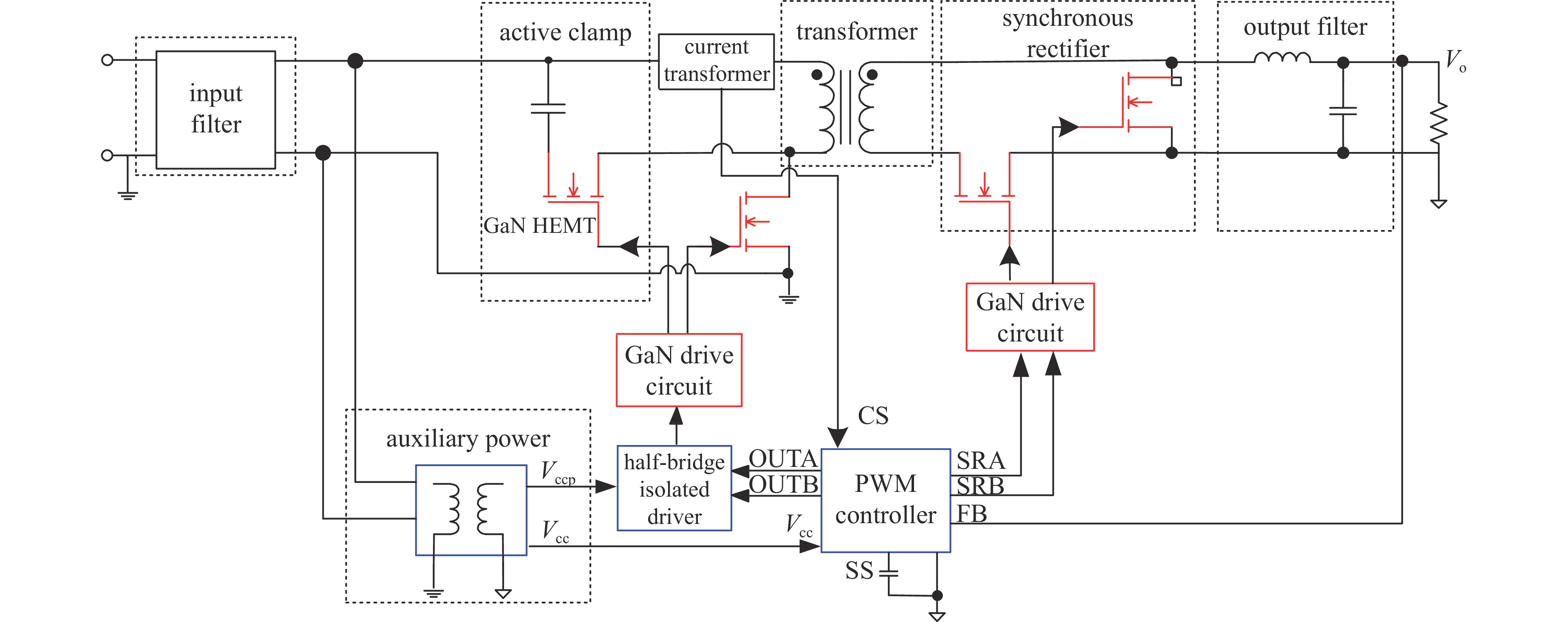
摘要: 混合集成DC-DC变换器因其工作温度范围宽和长期可靠性高在苛刻环境及高可靠需求应用场景中得到广泛应用。基于GaN HEMT器件优异的高频低损耗特性,结合有源箝位软开关拓扑、混合集成微组装技术和高载流低热阻气密封装技术,设计了一款28 V输入、5 V/20 A输出的混合集成DC-DC变换器。该变换器开关频率800 kHz,峰值效率达92%。详细阐述了有源箝位功率电路设计、GaN HEMT驱动电路寄生参数与震荡电压控制、同步整流时序与死区时间优化、厚膜混合集成工艺及散热的设计方法和技术细节,并通过仿真与样机实验,验证和展示了GaN HEMT和混合集成电路在高功率密度和高效率方面的优势。Abstract: Hybrid integrated DC-DC converters are widely used in harsh environments and applications with high-reliability requirements due to their wide operating temperature range and long-term reliability. This paper presents the design of a hybrid integrated DC-DC converter with an input voltage of 28 V and an output of 5 V/20 A, leveraging the excellent high-frequency, low-loss characteristics of gallium nitride (GaN) devices. The design incorporates an active clamp soft-switching topology, hybrid integrated micro-assembly technology, and high-current, low thermal resistance hermetic packaging techniques. The converter operates at a switching frequency of 800 kHz and achieves a peak efficiency of 92%. The paper elaborates in detail on the design methods and technical details of the active clamp power circuit, the control of parasitic parameters and oscillating voltage in the GaN HEMT drive circuit, the optimization of synchronous rectification timing and dead-time, the thick-film hybrid integration process, and heat dissipation design. Through simulations and prototype experiments, it verifies and demonstrates the advantages of GaN HEMTS and hybrid integrated circuits in high power density and high efficiency aspects.
-
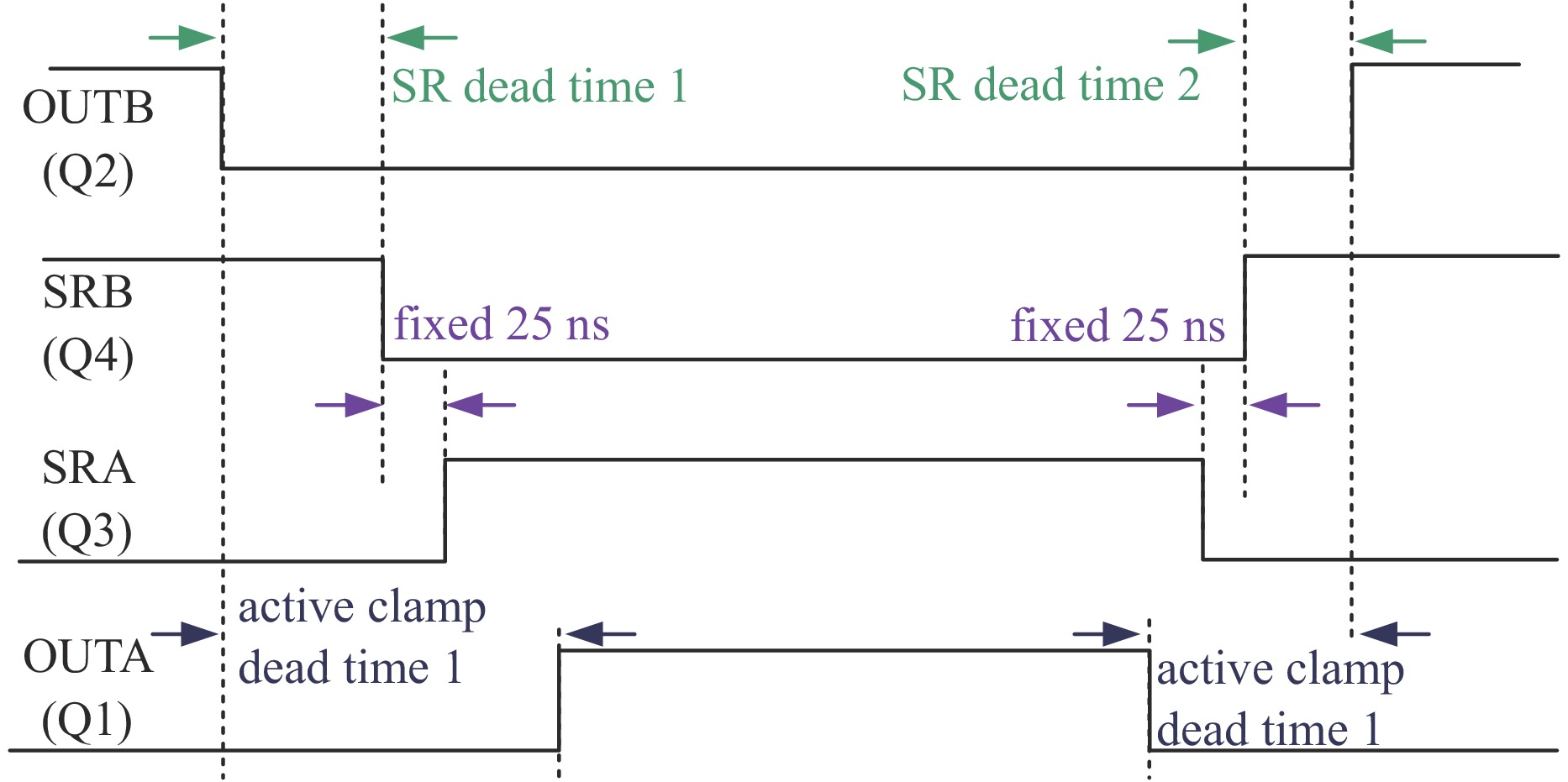
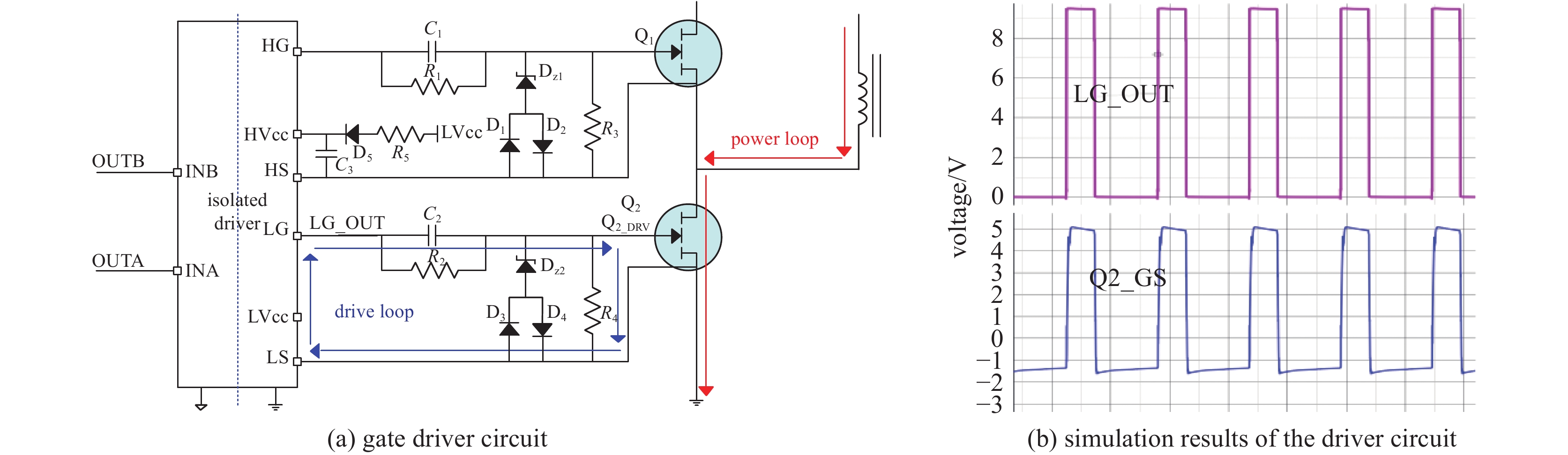
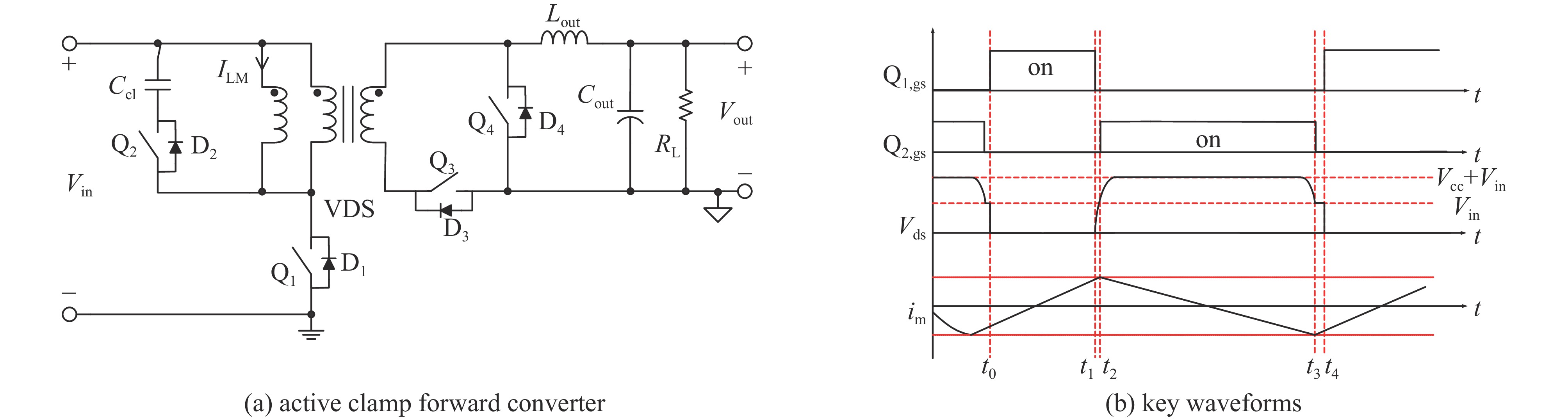
图 6 有源箝位及同步整流死区控制
Figure 6. Active clamp and synchronous rectification dead time control
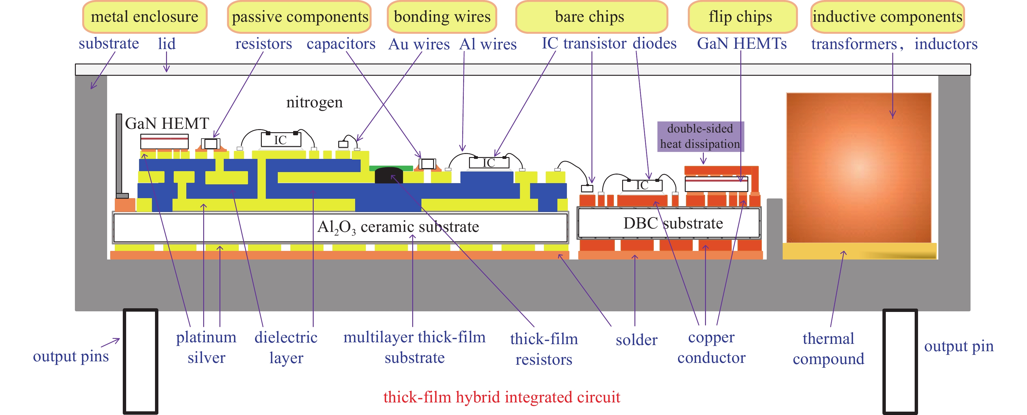
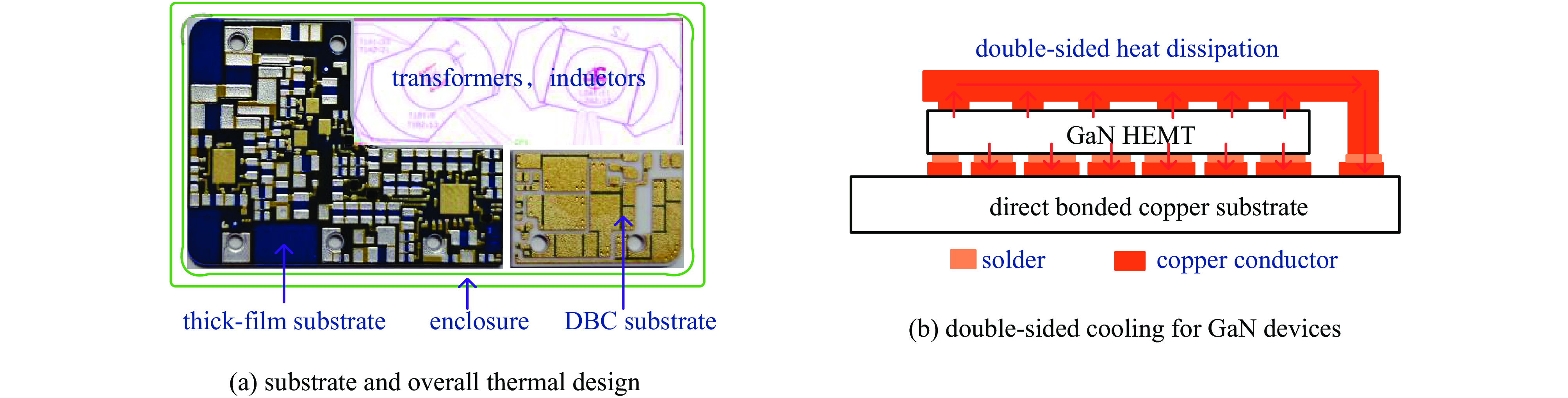
图 7 DC-DC变换器厚膜混合集成方案设计
Figure 7. Thick-film hybrid integrated circuit design for the DC-DC converter
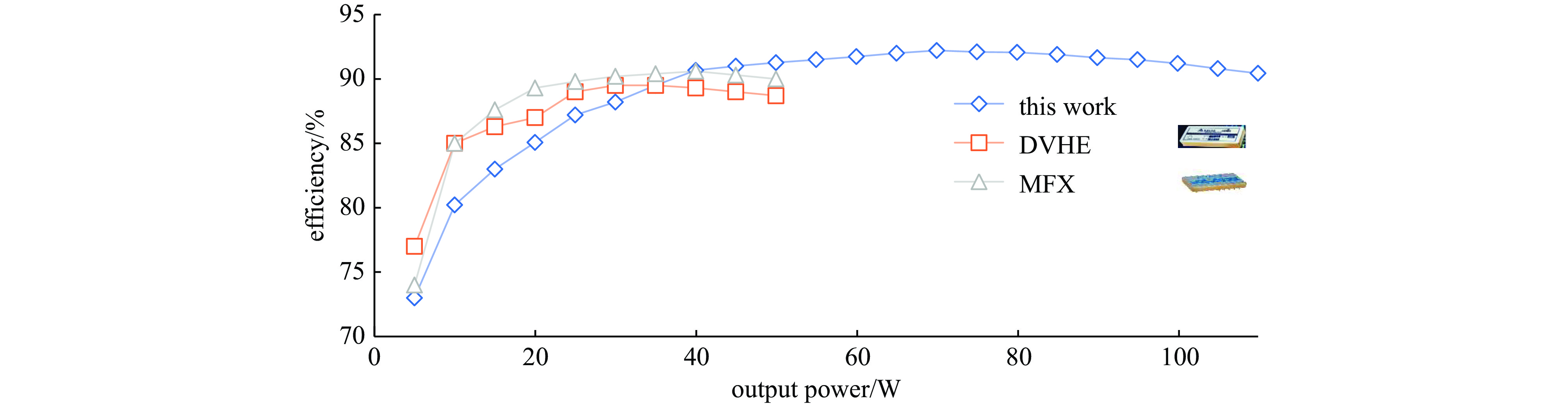
图 11 DC-DC变换器输出功率及效率对比
Figure 11. Comparison of output power and efficiency of DC-DC converters
表 1 开关管器件参数对比表
Table 1. Main device performance parameter comparison
device VDS,max/V ID/A RDS(on)/mΩ Qg/nC Coss/pF Qrr/nC dimensions/(mm×mm) SiR514DP 100 84.8 5 31 720 56 5.15×6.15 INN100W032A 100 60 3.2 9.2 460 0 3.5×2.13  下载: 导出CSV
-
[1] Wang Yang. Quality control of thick film hybrid integrated circuit process design and manufacturing[J]. Journal of Physics: Conference Series, 2021, 2037: 012008. doi: 10.1088/1742-6596/2037/1/012008 [2] 王浩. 厚膜混合集成电路封装互连材料和工艺研究[D]. 哈尔滨: 哈尔滨工业大学, 2014Wang Hao. Interconnect materials and processes for packaging thick film HIC[D]. Harbin: Harbin Institute of Technology, 2014 [3] Lidow A, d Rooij M, Strydom J, et al. GaN transistors for efficient power conversion[M]. 3rd ed. Hoboken: John Wiley & Sons Ltd, 2020. [4] Nguyen-Van Q, Pham-Nguyen L, Han H D, et al. Efficient GaN-based hybrid DC-DC converter with simple and low-cost bootstrap gate drivers for LED lighting applications[J]. AEU - International Journal of Electronics and Communications, 2022, 155: 154330. doi: 10.1016/j.aeue.2022.154330 [5] Rodríguez-Benítez O M, Ponce-Silva M, Aquí-Tapia J A, et al. Comparative performance and assessment study of a current-fed DC-DC resonant converter combining Si, SiC, and GaN-based power semiconductor devices[J]. Electronics, 2020, 9: 1982. doi: 10.3390/electronics9111982 [6] 佟强, 刘贺, 曲璐. 基于氮化镓的反激同步整流DC/DC变换器设计[J]. 电源学报, 2024, 22(2):81-89Tong Qiang, Liu He, Qu Lu. Design of synchronous rectifier flyback DC/DC converter based on GaN[J]. Journal of Power Supply, 2024, 22(2): 81-89 [7] 程哲. 第三代半导体材料及器件中的热科学和工程问题[J]. 物理学报, 2021, 70:236502Cheng Zhe. Thermal science and engineering in third-generation semiconductor materials and devices[J]. Acta Physica Sinica, 2021, 70: 236502 [8] 张宗烽. 先进封装系统中互连结构建模与GaN HEMT热分析方法研究[D]. 杭州: 杭州电子科技大学, 2023Zhang Zongfeng. Research on interconnect structure modeling and GaN HEMT thermal analysis methods in advanced packaging systems[D]. Hangzhou: Hangzhou Dianzi University, 2023 [9] 赵正平. GaN高频开关电力电子学的新进展[J]. 半导体技术, 2016, 41(1):1-9Zhao Zhengping. New advances in GaN high frequency switch power electronics[J]. Semiconductor Technology, 2016, 41(1): 1-9 [10] Li Xiaobin, Ma Hongbo, Yi Junhong, et al. A comparative study of GaN HEMT and Si MOSFET-based active clamp forward converters[J]. Energies, 2020, 13: 4160. doi: 10.3390/en13164160 [11] 崔梅婷. GaN器件的特性及应用研究[D]. 北京: 北京交通大学, 2015Cui Meiting. Research on characteristics and applications of GaN device[D]. Beijing: Beijing Jiaotong University, 2015 [12] Ghavidel Jalise M, Allahyari H, Shoaei A, et al. A self-driven synchronous rectification wide-range ZVS single-switch forward converter controlled using the variable inductance[J]. IET Power Electronics, 2023, 16(2): 320-332. doi: 10.1049/pel2.12386 [13] 王瑞东. 正激式有源箝位电压模开关电源的研究[D]. 西安: 西安电子科技大学, 2021Wang Ruidong. Research on forward active clamping voltage mode switching power supply[D]. Xi’an: Xidian University, 2021 [14] 陈伟, 李俊. 电源散热设计在高功率DC-DC变换器中的应用[J]. 电源学报, 2021, 19(4):52-60Chen Wei, Li Jun. Application of power dissipation design in high-power DC-DC converters[J]. Journal of Power Supply, 2021, 19(4): 52-60 [15] Kim N, Han C. Thermal analysis and design of a 75-W hybrid-type DC–DC converter for space applications[J]. Microelectronics Reliability, 2014, 54(8): 1555-1561. doi: 10.1016/j.microrel.2014.03.011 [16] Kumar V, Garg H, Singh C, et al. Mathematical and simulation analysis of natural convection heat transfer for DC–DC converter[J]. Proceedings of the Institution of Mechanical Engineers, Part C: Journal of Mechanical Engineering Science, 2020, 234(20): 4136-4146. doi: 10.1177/0954406220920318 -

 点击查看大图
计量
- 文章访问数: 942
- HTML全文浏览量: 254
- PDF下载量: 63
- 被引次数: 0
