

Response characteristics of intrinsic back-illuminated lateral silicon carbide photoconductive switches
-
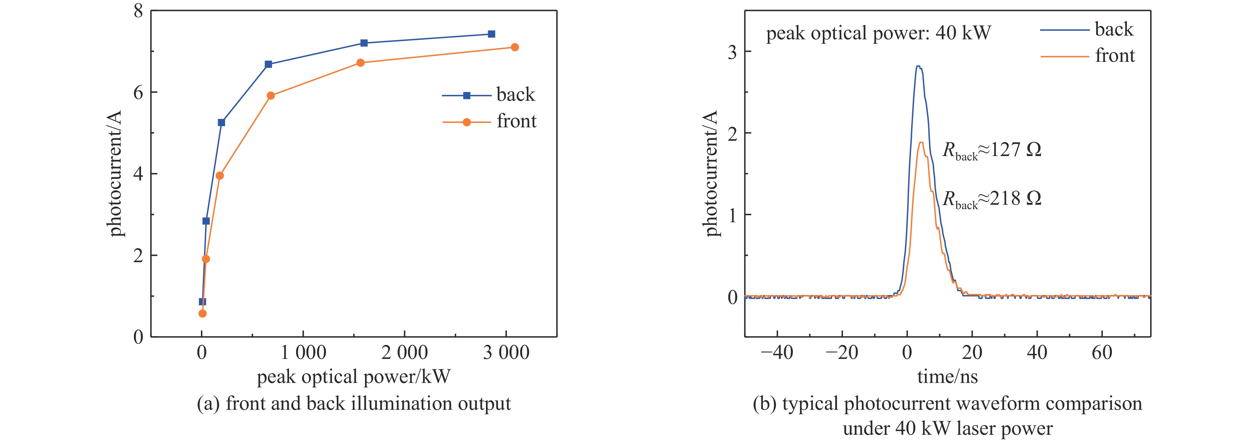
摘要: 平面碳化硅光导开关因可采用本征光触发而具有实现高光电增益的特点,但正面与背面光入射两种触发方式在响应特性上存在显著差异。基于TCAD数值仿真软件,对本征光背入射的平面碳化硅(SiC)光导开关的光电流响应进行研究,对比本征光触发下不同衬底厚度、不同光功率下器件正面与背面入光输出光电流,并对器件内部电流与电场分布状态进行对比分析,最终对厚度为50 μm的平面SiC光导开关进行了正面、背面触发实验测试。实验结果表明,40 kW峰值光功率下,与正面触发相比,背面触发器件的导通电阻减少了40%,验证了背面入光器件光电转换效率高的特点,且背面触发器件内部电场、电流更加均匀,更有利于提高器件高功率容量。结果为平面光导开关本征触发提供仿真与实验参考。Abstract: With the continuous development of photoconductive microwave technology towards high-frequency, high-power, long-life, and high-efficiency directions, lateral photoconductive devices have the potential to achieve high photoelectric gain and high main frequency response due to intrinsic light triggering and low parasitic capacitance. We investigated the photocurrent response of intrinsic light back-illuminated lateral silicon carbide (SiC) photoconductive switches. Based on semiconductor numerical simulation, the output photocurrent of the device under intrinsic light triggering with different substrate thicknesses and different light powers was compared for front and back illumination. The internal current and electric field distribution of the device were analyzed and compared. Finally, experimental tests were conducted on the front and back triggering of a 50 μm lateral SiC photoconductive switch. The experimental results show that under a 40 kW peak light power, the on-resistance of the back-triggered device is reduced by 40% compared to the front-triggered device, confirming the high photoelectric conversion efficiency of the back-illuminated device, and the internal electric field and current of the back-triggered device are more uniform, which is more conducive to improving the device’s high-power capacity. The results provide simulation and experimental references for the intrinsic triggering of planar photoconductive switches.
-
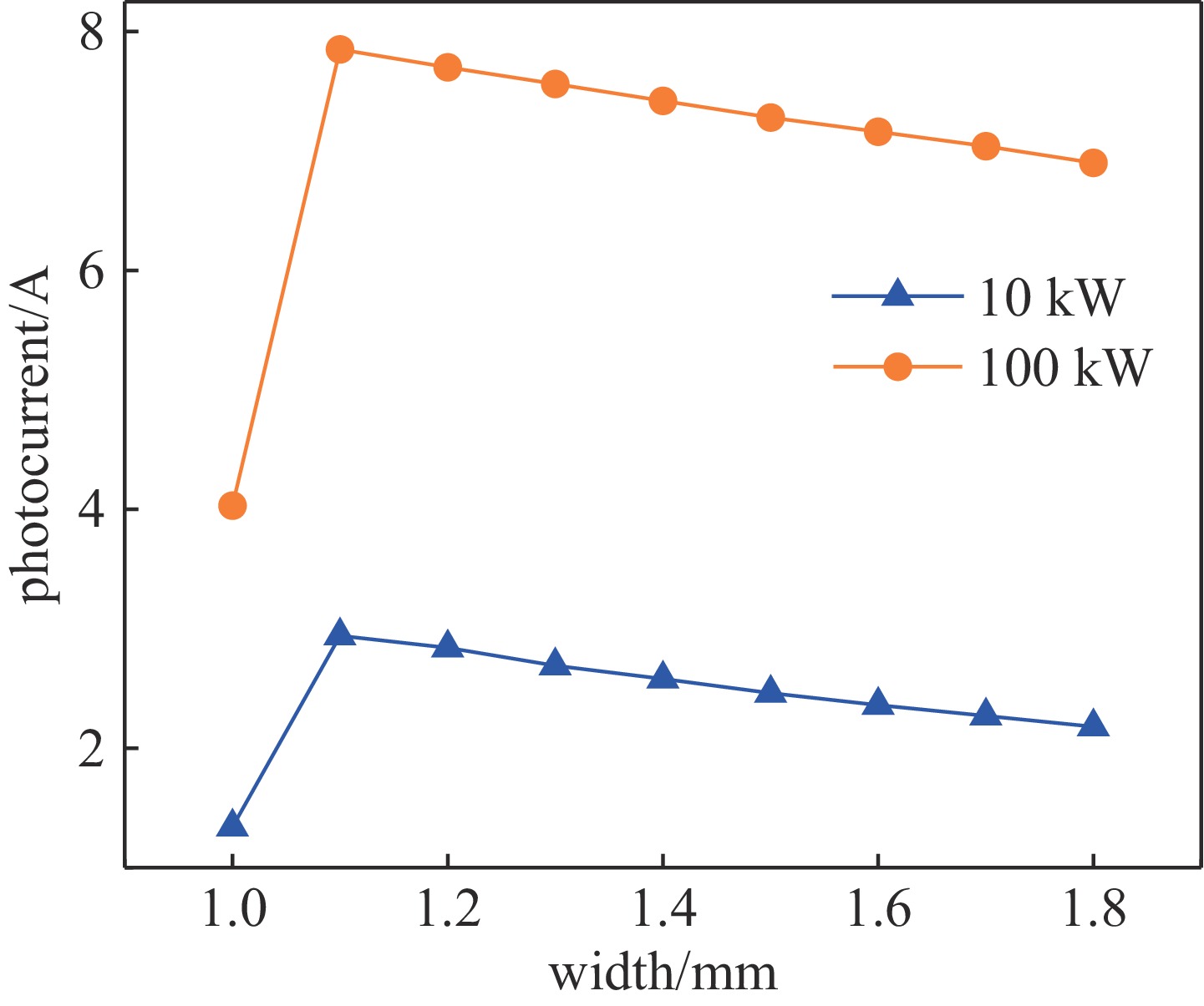
图 2 不同光束宽度下光电流输出对比图
Figure 2. Comparison of photocurrent output under different beam widths
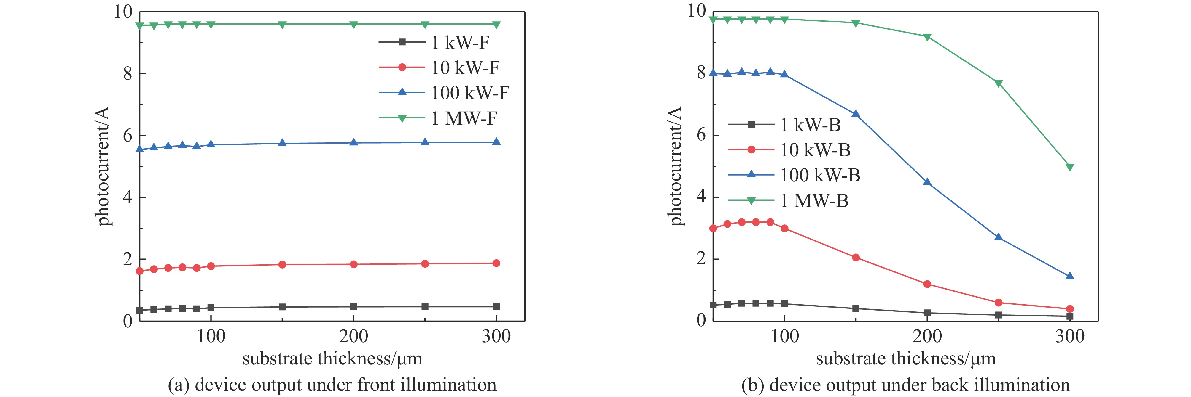
图 3 不同衬底厚度下正面与背面入光光电流幅值对比
Figure 3. Comparison of photocurrent amplitude under front and back illumination with different substrate thicknesses

图 4 10 kW峰值光功率下正面背面入光典型仿真波形与平面器件等效电路
Figure 4. Typical simulation waveforms under front and back illumination with a 10 kW peak optical power and equivalent circuit of planar devices
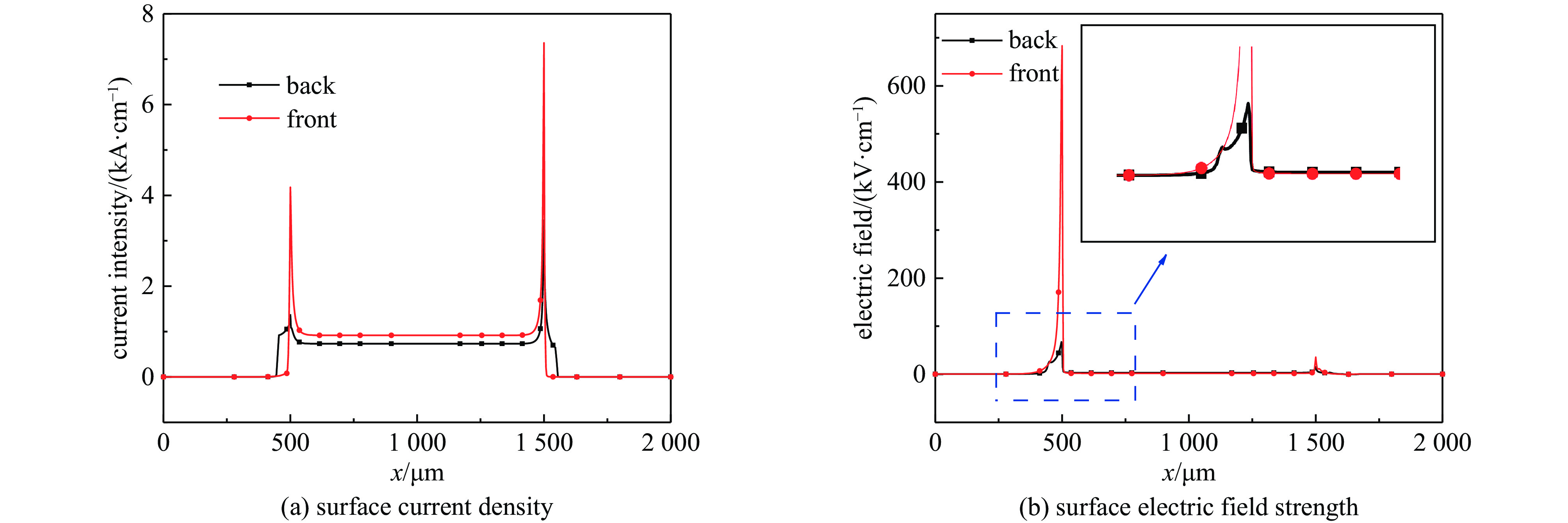
图 6 器件表面电流密度与电场强度对比
Figure 6. Comparison of surface current density and electric field intensity in devices
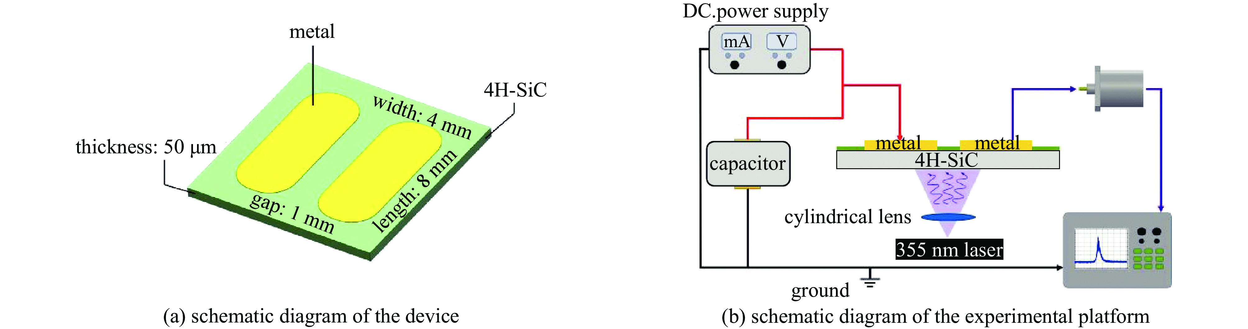
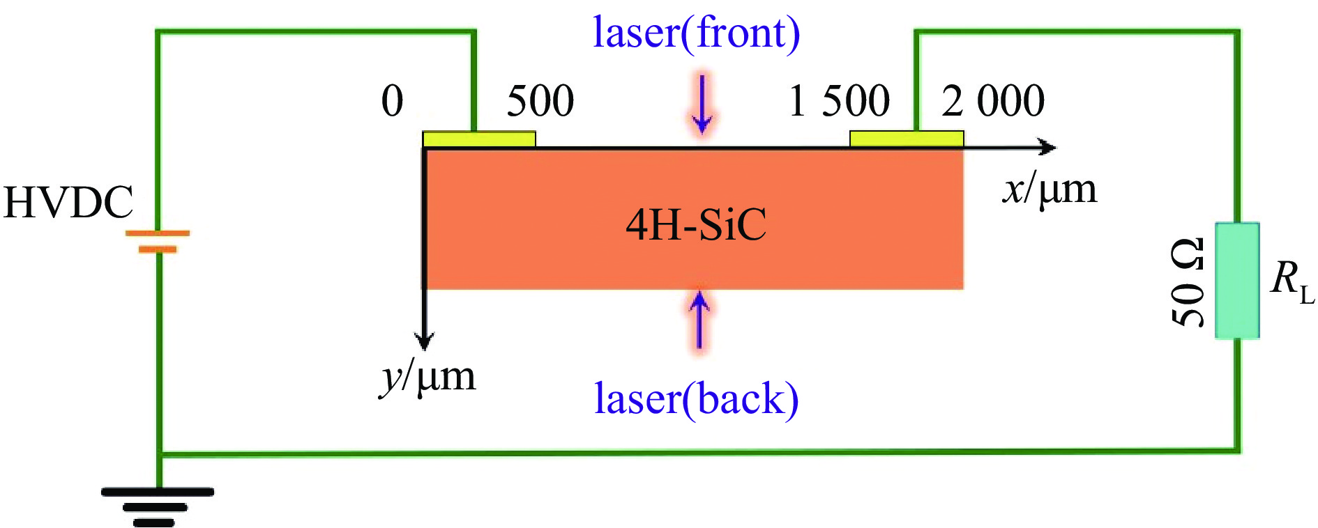
图 7 实验平台与测试器件示意图
Figure 7. Schematic diagram of the test device and the experimental platform
-
[1] 王朗宁. 碳化硅光导开关的初步研究[D]. 长沙: 国防科技大学, 2013Wang Langning. Preliminary study of silicon carbide photoconductive semiconductor switch[D]. Changsha: National University of Defense Technology, 2013 [2] 朱效庆, 荀涛, 王朗宁, 等. 一种推挽型光导微波放大器的电效率分析[J]. 现代应用物理, 2022, 13:010501 doi: 10.12061/j.issn.2095-6223.2022.010501Zhu Xiaoqing, Xun Tao, Wang Langning, et al. Electrical efficiency analysis of a push-pull photoconductive microwave amplifier[J]. Modern Applied Physics, 2022, 13: 010501 doi: 10.12061/j.issn.2095-6223.2022.010501 [3] Cai Ping, Jiang Lijuan, Xu Jiankai, et al. Design of a lateral photoconductive semiconductor switch with a low resistivity region on semi-insulating GaN to enhance breakdown characteristics[J]. Optics Communications, 2024, 555: 130232. doi: 10.1016/j.optcom.2023.130232 [4] Kirawanich P, Yakura S J, Islam N E. Study of high-power wideband terahertz-pulse generation using integrated high-speed photoconductive semiconductor switches[J]. IEEE Transactions on Plasma Science, 2009, 37(1): 219-228. doi: 10.1109/TPS.2008.2006978 [5] Mauch D, Sullivan W, Bullick A, et al. High power lateral silicon carbide photoconductive semiconductor switches and investigation of degradation mechanisms[J]. IEEE Transactions on Plasma Science, 2015, 43(6): 2021-2031. doi: 10.1109/TPS.2015.2424154 [6] Yang Xianghong, Hu Long, Liu Jingliang, et al. Si3N4 passivation and side illumination of high-power photoconductive semiconductor switch based on free-standing SI-GaN[J]. IEEE Transactions on Electron Devices, 2023, 70(3): 1128-1133. doi: 10.1109/TED.2023.3238362 [7] Xun Tao, Niu Xinyue, Wang Langning, et al. Recent progress of parameter-adjustable high-power photonic microwave generation based on wide-bandgap photoconductive semiconductors[J]. Chinese Optics Letters, 2024, 22: 012501. doi: 10.3788/COL202422.012501 [8] Niu Xinyue, Wu Qilin, Wang Bin, et al. Test of kW class photonic microwave generation using vanadium-compensated 6H-SiC PCSS and burst-mode-operation pulse laser[J]. IEEE Photonics Journal, 2023, 15: 5500407. [9] Zeng Linglong, Niu Xinyue, Liu Fuyin, et al. Dual-stacked SiC vertical photoconductive switch for modulation bandwidth extension of frequency-agile power microwave[J]. IEEE Electron Device Letters, 2024, 45(6): 992-995. doi: 10.1109/LED.2024.3386680 [10] Chu Xu, Xun Tao, Wang Langning, et al. Wide-range frequency-agile microwave generation up to 10 GHz based on vanadium-compensated 4H-SiC photoconductive semiconductor switch[J]. IEEE Electron Device Letters, 2022, 43(7): 1013-1016. doi: 10.1109/LED.2022.3179292 [11] Zhu K, Doğan S, Moon Y T, et al. Effect of n+-GaN subcontact layer on 4H–SiC high-power photoconductive switch[J]. Applied Physics Letters, 2005, 86: 261108. doi: 10.1063/1.1951056 [12] Feng Zhuoyun, Luan Chongbiao, Xiao Longfei, et al. Performance of a novel rear-triggered 4H-SiC photoconductive semiconductor switch[J]. IEEE Transactions on Electron Devices, 2023, 70(2): 627-632. doi: 10.1109/TED.2022.3227889 [13] Chu Xu, Meng Jin, Wang Haitao, et al. A backward-triggered 4H-SiC photoconductive semiconductor switch with planar electrode structure[J]. IEEE Transactions on Electron Devices, 2024, 71(7): 4253-4258. doi: 10.1109/TED.2024.3405470 [14] Hemmat Z, Faez R, Moreno E, et al. Transient and steady state study of a rear-illuminated 6H-SiC photoconductive semiconductor switch[J]. Optik, 2016, 127(11): 4615-4620. doi: 10.1016/j.ijleo.2016.01.174 [15] Rakheja S, Huang L, Hau-Riege S, et al. Performance modeling of silicon carbide photoconductive switches for high-power and high-frequency applications[J]. IEEE Journal of the Electron Devices Society, 2020, 8: 1118-1128. doi: 10.1109/JEDS.2020.3022031 [16] 伍麒霖. 基于线性光导器件的大功率微波产生技术研究[D]. 长沙. 国防科技大学, 2019Wu Qilin. Research on high power microwave generation technology based on linear photoconductive devices[D]. Changsha: National University of Defense Technology, 2019 -

 下载:
下载:

 点击查看大图
计量
- 文章访问数: 38
- HTML全文浏览量: 21
- PDF下载量: 1
- 被引次数: 0
