

Preliminary development and high-voltage lifetime testing of vertical photoconductive semiconductor switches based on Fe-doped β-Ga2O3
-
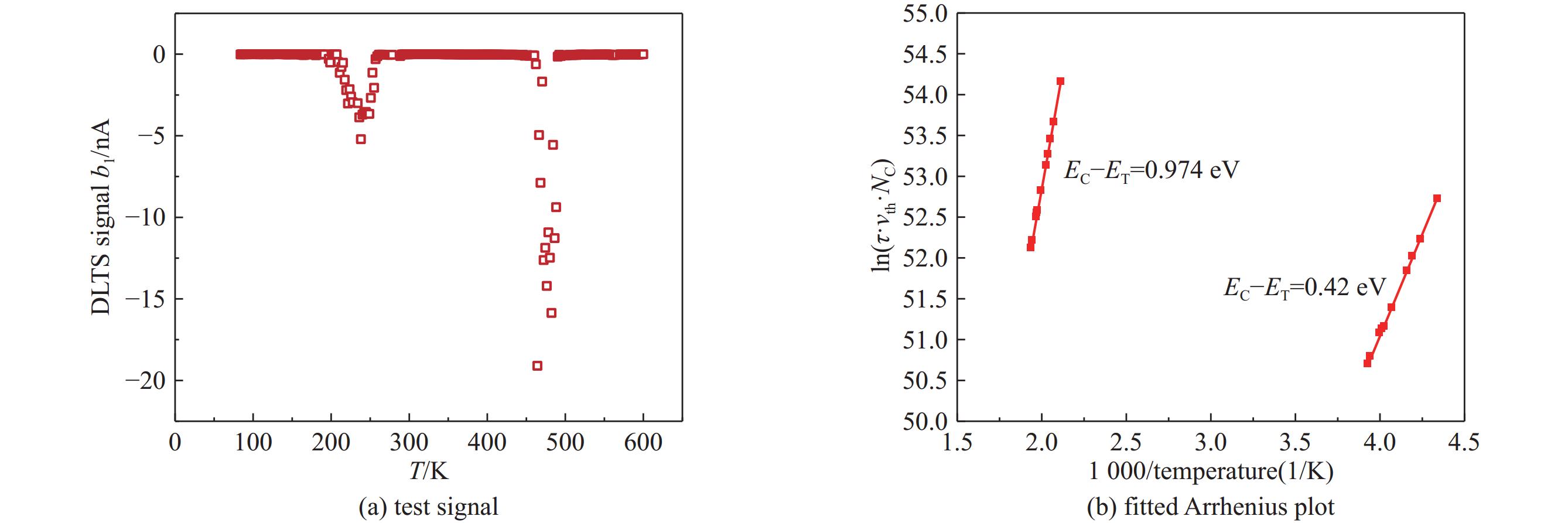
摘要: 主要围绕Fe: β-Ga2O3基垂直型光导开关的高压性能进行实验和分析。结果显示,Fe: β-Ga2O3中深能级能提供产生非本征激发的载流子,输入电压为20 kV并进行单次激光触发时器件未出现击穿趋势,在15 kV下以10 Hz光触发至少
5000 余次后开关损坏,有效数据中脉冲表现较为稳定,初步证明了氧化镓光导开关可应用于大功率和高频等极限环境。失效分析说明较大的禁带宽度不是决定高耐压的唯一条件,除了使用精确掺杂的手段引入特定缺陷来改变Ga2O3材料性能外,进一步改良现有的材料生长方式和器件封装结构等也对提高光导开关的输出和寿命有所帮助。Abstract: This study focuses on the performance of vertical photoconductive semiconductor switch (PCSS) based on Fe: β-Ga2O3 under high voltage. The results show that deep levels in Fe: β-Ga2O3 can provide carriers of non-intrinsic excitation. The device did not exhibit breakdown tendencies when subjected to a 20 kV input voltage with single-shot laser triggering. After more than5000 trigger cycles at 15 kV by a 10 Hz laser, the switch eventually failed. Nevertheless, pulse performance remained stable throughout the effective data collection period, preliminarily demonstrating the potential of Ga2O3 PCSS for applications in extreme conditions such as high power and high frequency. Failure analysis indicates that a wide bandgap is not the sole determinant of high breakdown voltage. In addition to employing precise doping techniques to introduce specific defects and modify material properties, further improvements in existing material growth methods and device packaging structures can also contribute to enhancing the output and lifetime of PCSS.-
Key words:
- β-Ga2O3 /
- deep level /
- PCSS /
- reliability /
- pulse power
-

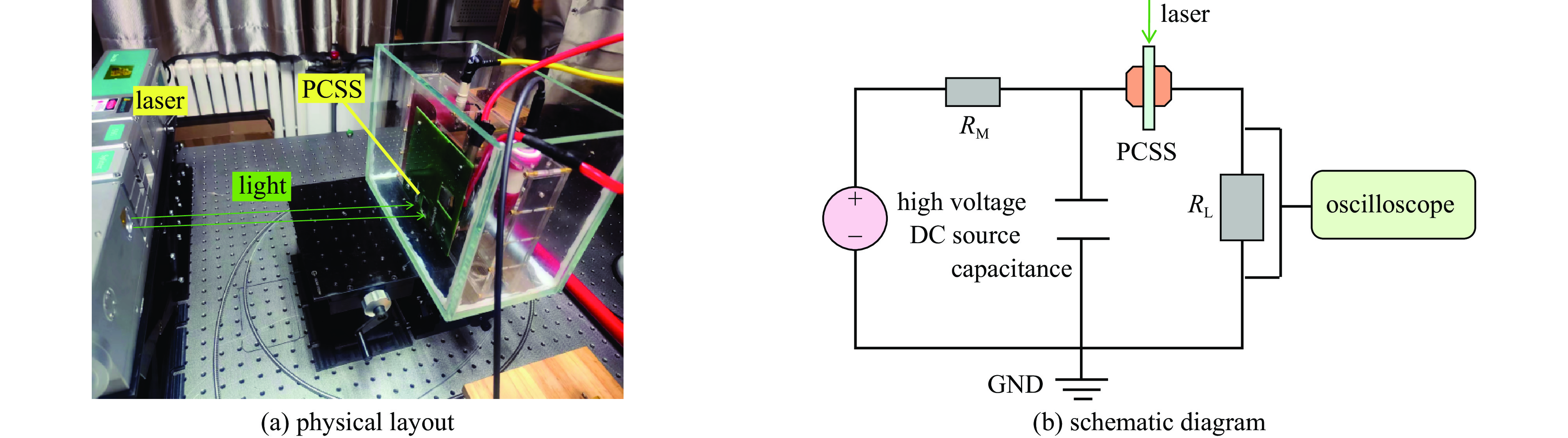
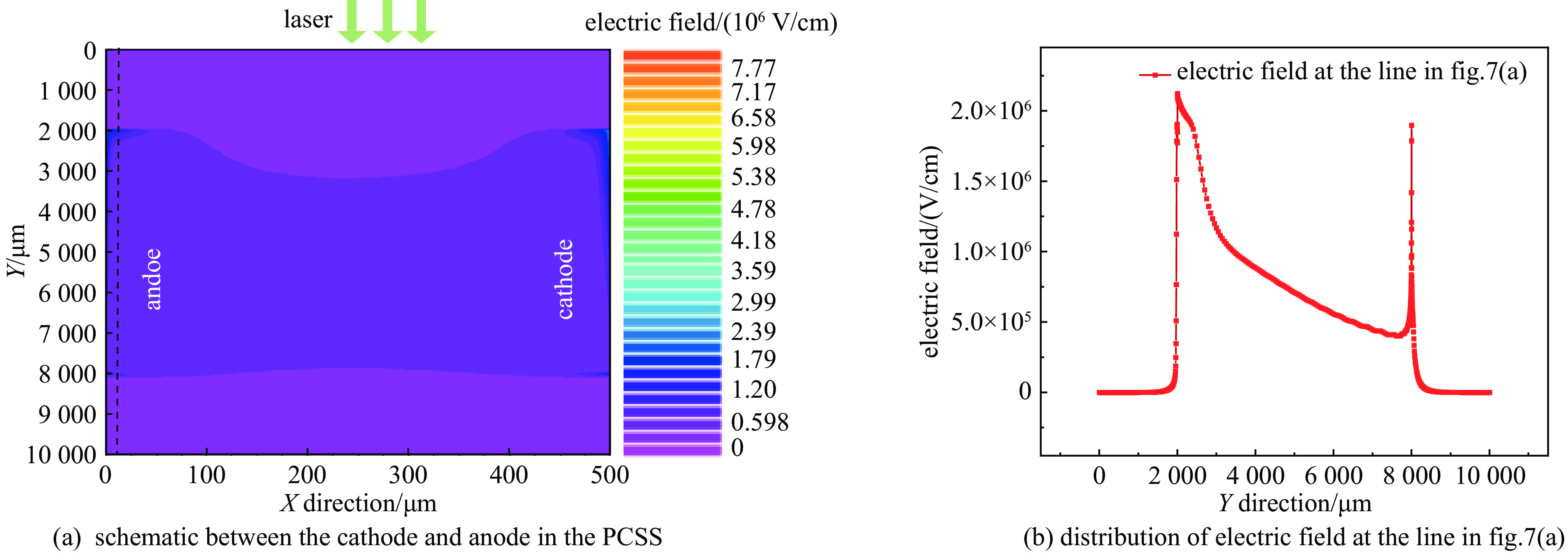
图 1 氧化镓和铜电极封装成的光导开关
Figure 1. PCSS fabricated by encapsulating gallium oxide with copper electrodes
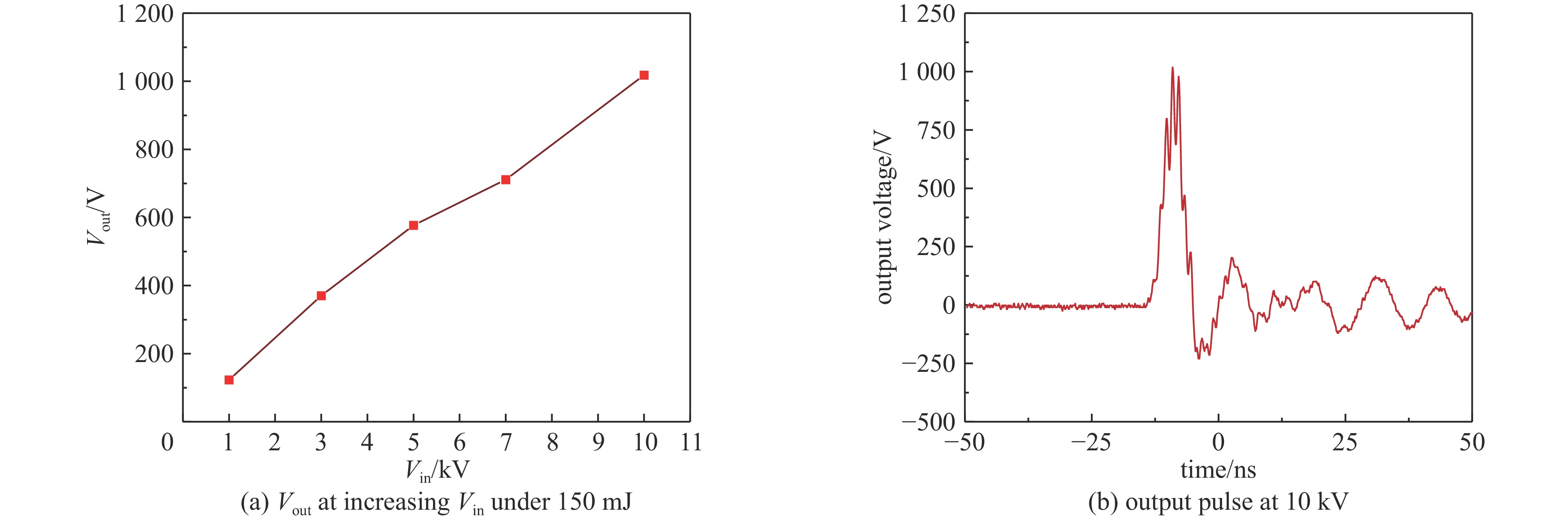
图 4 实验一结果:单次光触发下递增输入电压的最大输出与输出脉冲展示
Figure 4. Maximum output under increasing input voltage and output pulse at 10 kV of experiment 1
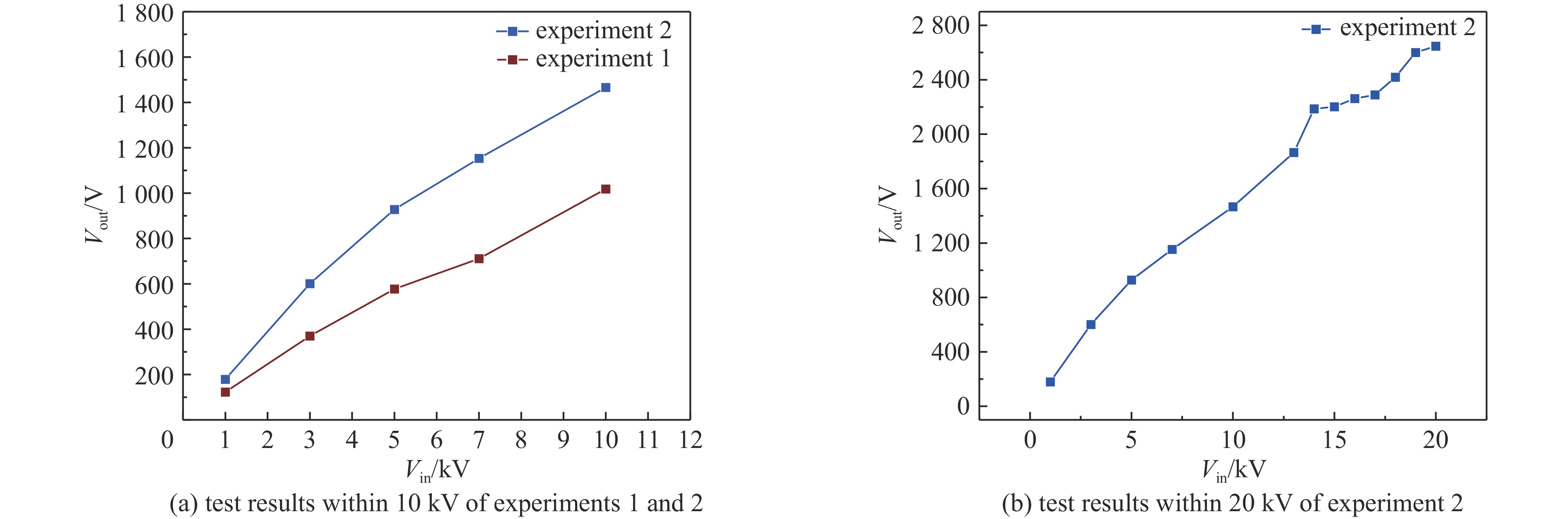
图 5 实验2结果及其部分结果与实验1的对比
Figure 5. Results of experiment 2 with comparative analysis against experiment 1
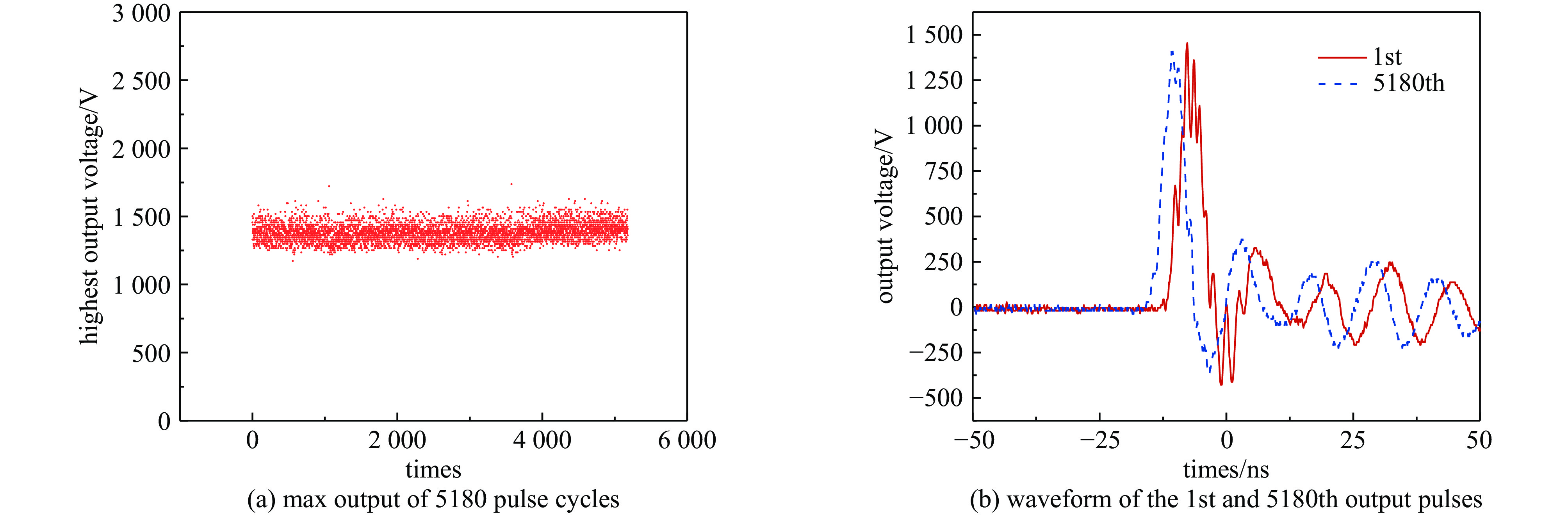
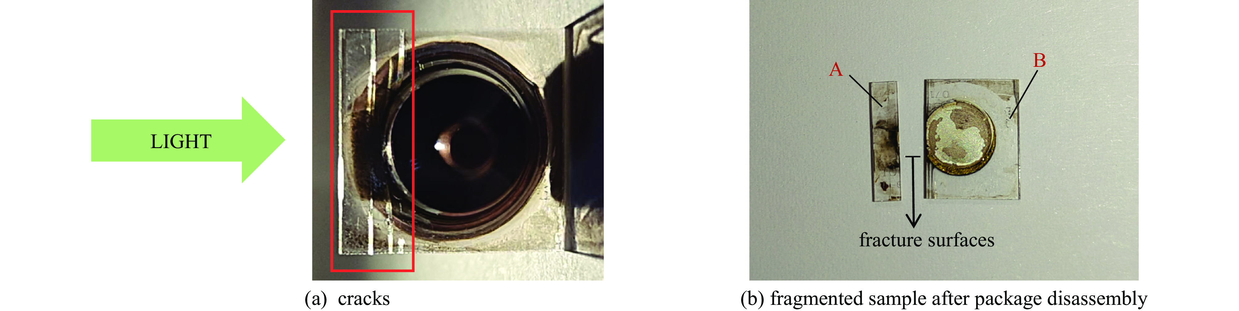
图 6 实验
5180 次脉冲的最大输出与首末两次输出脉冲对比Figure 6. Maximum output of
5180 pulse and the 1st and 5,180th output pulses表 1 主要半导体材料迁移率[5]
Table 1. Carrier mobility in principal semiconductor materials
mobility(μ/cm2·V−1·s−1) Si Ge GaAs 4H-SiC GaN β-Ga2O3 diamond(C) hole 300 1900 100~ 3000 90 10 8 3800 electron 1480 3900 8400 1000 1200 300 4500  下载: 导出CSV
表 2 四个观测点的EDS结果
Table 2. EDS results at 4 spots
atom percentage/% Ga O C EDS spot1 11.05 8.88 67.20 EDS spot2 24.76 13.40 61.65 EDS spot3 44.62 16.58 38.80 EDS spot4 36.64 17.25 46.11
下载: 导出CSV
-
[1] Roy R, Hill V G, Osborn E F. Polymorphism of Ga2O3 and the system Ga2O3-H2O[J]. Journal of the American Chemical Society, 1952, 74(3): 719-722. doi: 10.1021/ja01123a039 [2] Pearton S J, Yang Jiancheng, Cary P H, et al. A review of Ga2O3 materials, processing, and devices[J]. Applied Physics Reviews, 2018, 5: 011301. doi: 10.1063/1.5006941 [3] Onuma T, Fujioka S, Yamaguchi T, et al. Correlation between blue luminescence intensity and resistivity in β-Ga2O3 single crystals[J]. Applied Physics Letters, 2013, 103: 041910. doi: 10.1063/1.4816759 [4] 崔慧源. β-Ga2O3单晶导电机理研究与缺陷能级分析[D]. 上海: 上海大学, 2020: 1-11Cui Huiyuan. Conduction mechanism study and defect level analysis of β-Ga2O3 single crystal[D]. Shanghai: Shanghai University, 2020: 1-11 [5] 周磊簜, 陈亮, 卢星, 等. 氧化镓半导体核辐射探测器研究现状[J]. 现代应用物理, 2022, 13:010101 doi: 10.12061/j.issn.2095-6223.2022.010101Zhou Leidang, Chen Liang, Lu Xing, et al. Research status of gallium oxide(Ga2O3) semiconductor nuclear radiation detectors[J]. Modern Applied Physics, 2022, 13: 010101 doi: 10.12061/j.issn.2095-6223.2022.010101 [6] Yan Xiaodong, Esqueda I S, Ma Jiahui, et al. High breakdown electric field in β-Ga2O3/graphene vertical barristor heterostructure[J]. Applied Physics Letters, 2018, 112: 032101. doi: 10.1063/1.5002138 [7] Pratiyush A S, Muazzam U U, Kumar S, et al. Optical float-zone grown bulk β-Ga2O3-based linear MSM array of UV-C photodetectors[J]. IEEE Photonics Technology Letters, 2019, 31(12): 923-926. doi: 10.1109/LPT.2019.2913286 [8] He Nuotian, Tang Huili, Liu Bo, et al. Ultra-fast scintillation properties of β-Ga2O3 single crystals grown by floating zone method[J]. Nuclear Instruments and Methods in Physics Research Section A: Accelerators, Spectrometers, Detectors and Associated Equipment, 2018, 888: 9-12. [9] Galazka Z, Irmscher K, Schewski R, et al. Czochralski-grown bulk β-Ga2O3 single crystals doped with mono-, di-, tri-, and tetravalent ions[J]. Journal of Crystal Growth, 2020, 529: 125297. doi: 10.1016/j.jcrysgro.2019.125297 [10] Jesenovec J, Varley J, Karcher S E, et al. Electronic and optical properties of Zn-doped β-Ga2O3 Czochralski single crystals[J]. Journal of Applied Physics, 2021, 129: 225702. doi: 10.1063/5.0050468 [11] Aida H, Nishiguchi K, Takeda H, et al. Growth of β-Ga2O3 single crystals by the edge-defined, film fed growth method[J]. Japanese Journal of Applied Physics, 2008, 47: 8506. doi: 10.1143/JJAP.47.8506 [12] Masuya S, Sasaki K, Kuramata A, et al. Characterization of crystalline defects in β-Ga2O3 single crystals grown by edge-defined film-fed growth and halide vapor-phase epitaxy using synchrotron X-ray topography[J]. Japanese Journal of Applied Physics, 2019, 58: 055501. doi: 10.7567/1347-4065/ab0dba [13] Mu Wenxiang, Jia Zhitai, Yin Yanru, et al. High quality crystal growth and anisotropic physical characterization of β-Ga2O3 single crystals grown by EFG method[J]. Journal of Alloys and Compounds, 2017, 714: 453-458. doi: 10.1016/j.jallcom.2017.04.185 [14] Zhang Shengnan, Lian Xiaozheng, Ma Yanchao, et al. Growth and characterization of 2-inch high quality β-Ga2O3 single crystals grown by EFG method[J]. Journal of Semiconductors, 2018, 39: 083003. doi: 10.1088/1674-4926/39/8/083003 [15] Hoshikawa K, Ohba E, Kobayashi T, et al. Growth of β-Ga2O3 single crystals using vertical Bridgman method in ambient air[J]. Journal of Crystal Growth, 2016, 447: 36-41. doi: 10.1016/j.jcrysgro.2016.04.022 [16] 董林鹏. 氧化镓材料特性及光电探测器研究[D]. 西安: 西安电子科技大学, 2019Dong Linpeng. Study on characteristics of gallium oxide material and photodetectors[D]. Xi’an: Xidian University, 2019 [17] Yadav S, Dash S, Patra A K, et al. Effects of energetic ion irradiation on β-Ga2O3 thin films[J]. ECS Journal of Solid State Science and Technology, 2020, 9: 045015. [18] Mauch D, Sullivan W, Bullick A, et al. High power lateral silicon carbide photoconductive semiconductor switches and investigation of degradation mechanisms[J]. IEEE transactions on plasma science, 2015, 43(6): 2021-2031. [19] 郝跃. 宽禁带与超宽禁带半导体器件新进展[J]. 科技导报, 2019, 37(3):58-61Hao Yue. New progress in wide and ultra-wide bandgap semiconductor devices[J]. Science & Technology Review, 2019, 37(3): 58-61 [20] 洪旭. β-Ga2O3基光导开关器件建模与实验研究[D]. 西安: 西安电子科技大学, 2022: 1-15Hong Xu. Study on modeling and experimental of β-Ga2O3 photoconductive semiconductor switch[D]. Xi’an: Xidian University, 2022: 1-15 [21] Jayaraman S, Lee C H. Observation of two-photon conductivity in GaAs with nanosecond and picosecond light pulses[J]. Applied Physics Letters, 1972, 20(10): 392-395. doi: 10.1063/1.1653989 [22] Auston D H, Shank C V, LeFur P. Picosecond optical measurements of band-to-band Auger recombination of high-density plasmas in germanium[J]. Physical Review Letters, 1975, 35(15): 1022-1025. doi: 10.1103/PhysRevLett.35.1022 [23] LeFur P, Auston D H. A kilovolt picosecond optoelectronic switch and Pockel’s cell[J]. Applied Physics Letters, 1976, 28(1): 21-23. doi: 10.1063/1.88565 [24] 严成锋, 施尔畏, 陈之战, 等. 超快大功率SiC光导开关的研究[J]. 无机材料学报, 2008, 23(3):425-428 doi: 10.3321/j.issn:1000-324X.2008.03.002Yan Chengfeng, Shi Erwei, Chen Zhizhan, et al. Super fast and high power SiC photoconductive semiconductor switches[J]. Journal of Inorganic Materials, 2008, 23(3): 425-428 doi: 10.3321/j.issn:1000-324X.2008.03.002 [25] Dowling K M, Chatterjee B, Ghandiparsi S, et al. Evaluation of Fe-βGa2O3 for photoconductive semiconductor switching[J]. IEEE Transactions on Electron Devices, 2024, 71(3): 1535-1540. doi: 10.1109/TED.2024.3352528 [26] 张乃霁. Fe: β-Ga2O3单晶的微观结构及光学电学性能研究[D]. 南宁: 广西大学, 2021: 1-13Zhang Naiji. Study on optical and electrical properties of Fe: β-Ga2O3 single crystal and microstructure characteristic[D]. Nanning: Guangxi University, 2021: 1-13 [27] Zhang Hao, Tang Huili, He Nuotian, et al. Growth and physical characterization of high resistivity Fe: β-Ga2O3 crystals[J]. Chinese Physics B, 2020, 29: 087201. [28] Hany I, Yang Ge, Chung C C. Fast X-ray detectors based on bulk β-Ga2O3 (Fe)[J]. Journal of Materials Science, 2020, 55(22): 9461-9469. [29] Chu Xu, Meng Jin, Wang Haitao, et al. A backward-triggered 4H-SiC photoconductive semiconductor switch with planar electrode structure[J]. IEEE Transactions on Electron Devices, 2024, 71(7): 4253-4258. [30] Seebauer E G, Kratzer M C. Charged point defects in semiconductors[J]. Materials Science and Engineering: R: Reports, 2006, 55(3/6): 57-149. [31] 迪特尔·K·施罗德, 徐友龙, 任巍, 等. 半导体材料与器件表征[M]. 3版. 西安: 西安交通大学出版社, 2017: 222-262Schroder D K, Xu Youlong, Ren Wei, et al. Semiconductor material and device characterization[M]. 3rd ed. Xi’an: Xi’an Jiaotong University Press, 2017: 222-262 [32] Farzana E, Mauze A, Varley J B, et al. Influence of neutron irradiation on deep levels in Ge-doped (010) β-Ga2O3 layers grown by plasma-assisted molecular beam epitaxy[J]. APL Materials, 2019, 7: 121102. doi: 10.1063/1.5126463 [33] Irmscher K, Galazka Z, Pietsch M, et al. Electrical properties of β-Ga2O3 single crystals grown by the Czochralski method[J]. Journal of Applied Physics, 2011, 110: 0637200. [34] Farzana E, Chaiken M F, Blue T E, et al. Impact of deep level defects induced by high energy neutron radiation in β-Ga2O3[J]. APL Materials, 2019, 7: 022502. doi: 10.1063/1.5054606 [35] Arehart A R, Ringel S A. Electrical properties 3[M]//Higashiwaki M, Fujita S. Gallium Oxide: Materials Properties, Crystal Growth, and Devices. Cham: Springer, 2020: 421-441. [36] 宋涛. 氧化镓薄膜忆阻器的热稳定性研究[D]. 西安: 西安电子科技大学, 2023Song Tao. Study on thermal stability of memristor based on gallium oxide film[D]. Xi’an: Xidian University, 2023 [37] Sun Qian, Guo Hui, Zheng Zhong, et al. Influence of pinch effect on the lifetime of a 2MW silicon carbide photoconductive semiconductor switch[J]. IEEE Transactions on Electron Devices, 2024, 71(3): 2018-2023. doi: 10.1109/TED.2024.3351100 -


 点击查看大图
计量
- 文章访问数: 78
- HTML全文浏览量: 41
- PDF下载量: 19
- 被引次数: 0
