

Effects of electromagnetic pulse and single event effect on electrical characteristics of SOI MOSFET
-
摘要: SOI MOSFET器件广泛应用于航天电子设备中,但它们容易受到空间中电磁脉冲及粒子辐照效应的影响,进而影响航天器的稳定性。通过建立二维的短沟道SOI MOSFET器件模型,探究电磁脉冲和重离子辐照引起的单粒子效应对器件电学特性的影响。研究结果表明,在电磁脉冲作用下,随着电磁脉冲电压幅值的增大,SOI MOSFET会发生雪崩击穿,雪崩击穿现象导致PN结内建电场的电场强度和电流密度的增加,继而导致晶格温度上升;器件发生雪崩击穿的阈值电压随着栅极电压的增加而降低,同时也随着源极和漏极之间沟道长度的减小而降低。重离子入射会使SOI MOSFET器件的瞬态漏电流激增,随着电子-空穴对的复合和扩散,电流逐渐减小。电磁脉冲和重离子协同作用于器件时,重离子辐照降低了器件发生雪崩击穿的阈值电压。Abstract:
Background In space environments, electronic systems are vulnerable to various adverse effects, including electromagnetic pulses (EMP) and particle radiation, which can significantly degrade device performance and reliability. Silicon-On-Insulator (SOI) MOSFETs are widely used in aerospace applications due to their excellent electrical characteristics, but their response to combined radiation effects needs further investigation.Purpose This study aims to analyze the effects of electromagnetic pulses and heavy-ion induced single-particle events on the electrical characteristics of short-channel SOI MOSFETs. It also explores the synergistic impact when both effects occur simultaneously, providing insights for improving device robustness in harsh space conditions.Methods A two-dimensional TCAD-based numerical model of short-channel SOI MOSFETs was developed, incorporating impact ionization, carrier generation and recombination, heat transfer, and thermodynamic effects. Electromagnetic pulses were modeled as transient voltage pulses with varying amplitudes, while heavy-ion effects were simulated through charge deposition profiles characterized by LET parameters. The influence of gate voltage, channel length, and LET on device behavior was systematically studied.Results Simulation results indicate that EMP-induced voltage transients can cause avalanche breakdown in the drain PN junction, with breakdown voltage decreasing as gate bias increases or channel length shortens. The internal electric field, current density, and device temperature intensify during breakdown. Heavy-ion irradiation generates electron-hole pairs, causing transient increases in drain current, which lower the avalanche breakdown threshold when combined with EMP. Higher LET values further exacerbate device degradation by increasing ionization effects and reducing breakdown voltages. The combined effects produce more severe electrical deterioration compared to single effects.Conclusions The research demonstrates that both EMP and heavy-ion irradiation can markedly weaken the electrical stability of short-channel SOI MOSFETs. These findings underscore the importance of designing radiation-hardened devices for space applications. The study provides a theoretical basis for future investigations into the synergistic effects of radiation phenomena on power semiconductor devices.-
Key words:
- MOSFET /
- electromagnetic pulse /
- single event effect /
- avalanche breakdown /
- simulation modeling
-
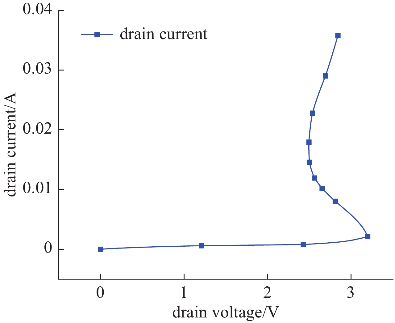
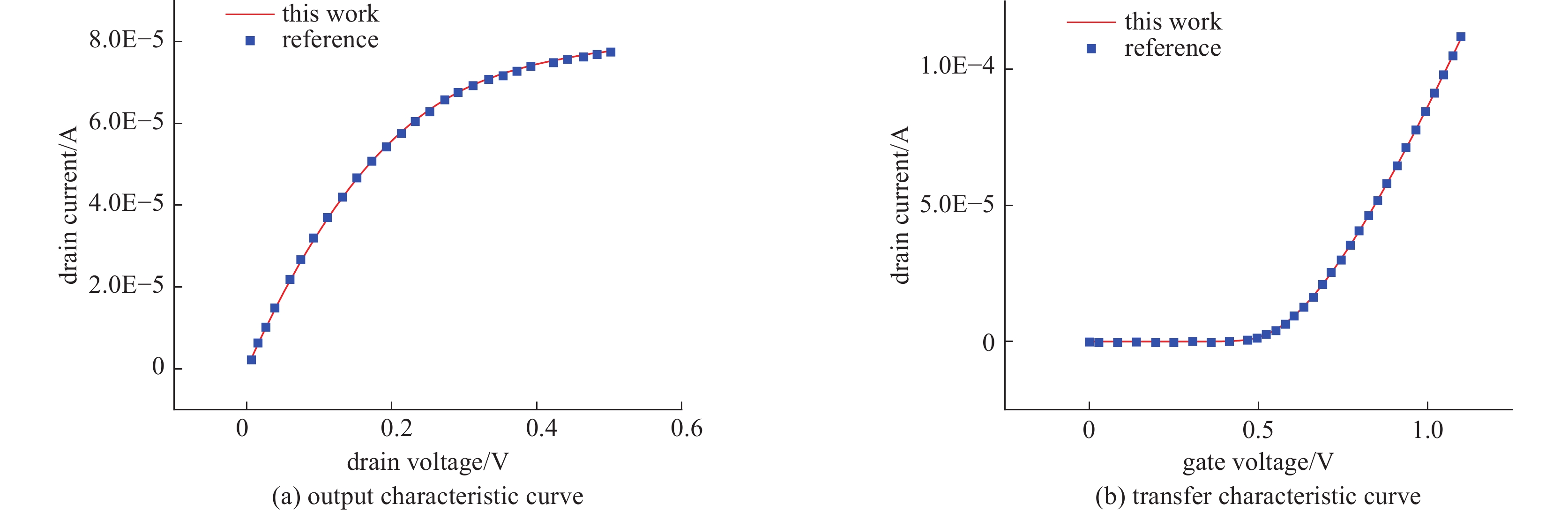
图 5 电磁脉冲作用下MOSFET输出特性曲线
Figure 5. Output characteristic curve of mosfet under electromagnetic pulse action
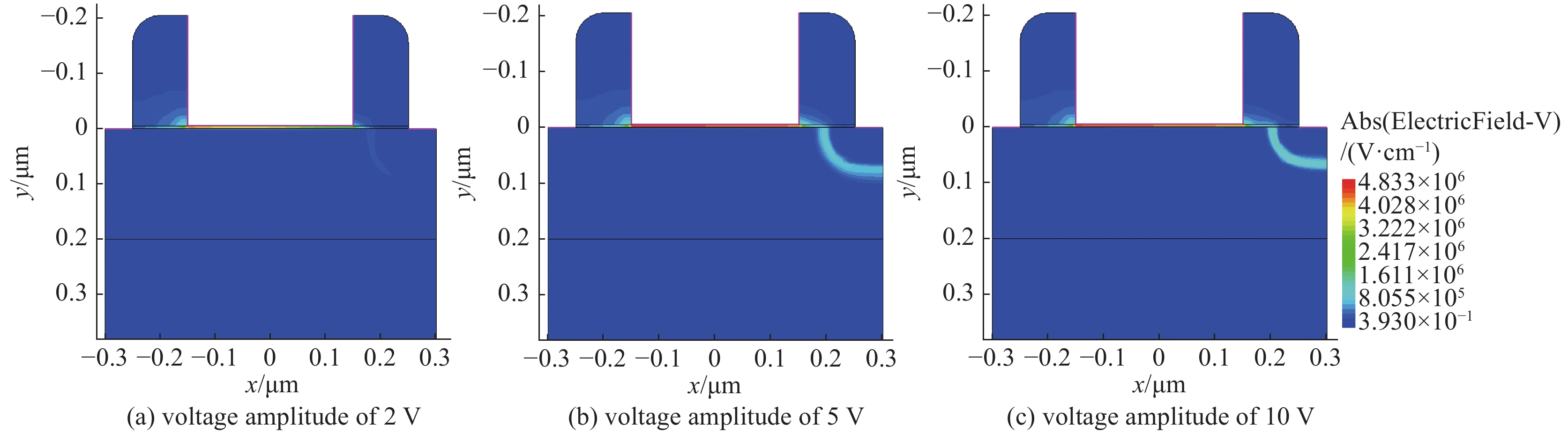
图 6 脉冲电压幅值分别为2 V、5 V和10 V时器件电场强度分布
Figure 6. Electric field distribution of the device at pulse voltage amplitudes of 2 V, 5 V, and 10 V
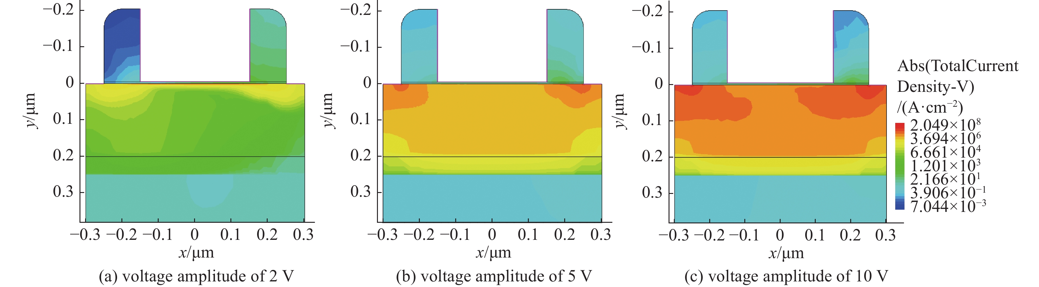
图 7 脉冲电压幅值分别为2 V、5 V和10 V时器件总电流密度分布
Figure 7. Total current density distribution of the device at pulse voltage amplitudes of 2 V, 5 V, and 10 V
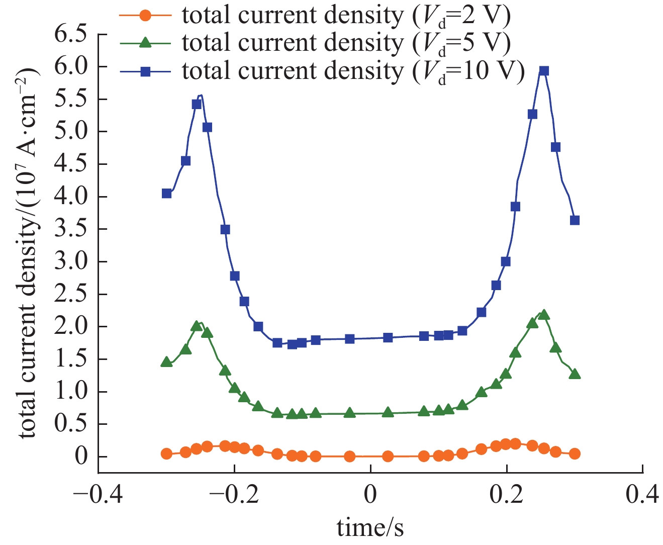
图 8 y=0.017 μm处横轴上总电流密度分布
Figure 8. Total current density distribution on the horizontal axis at y = 0.017 μm
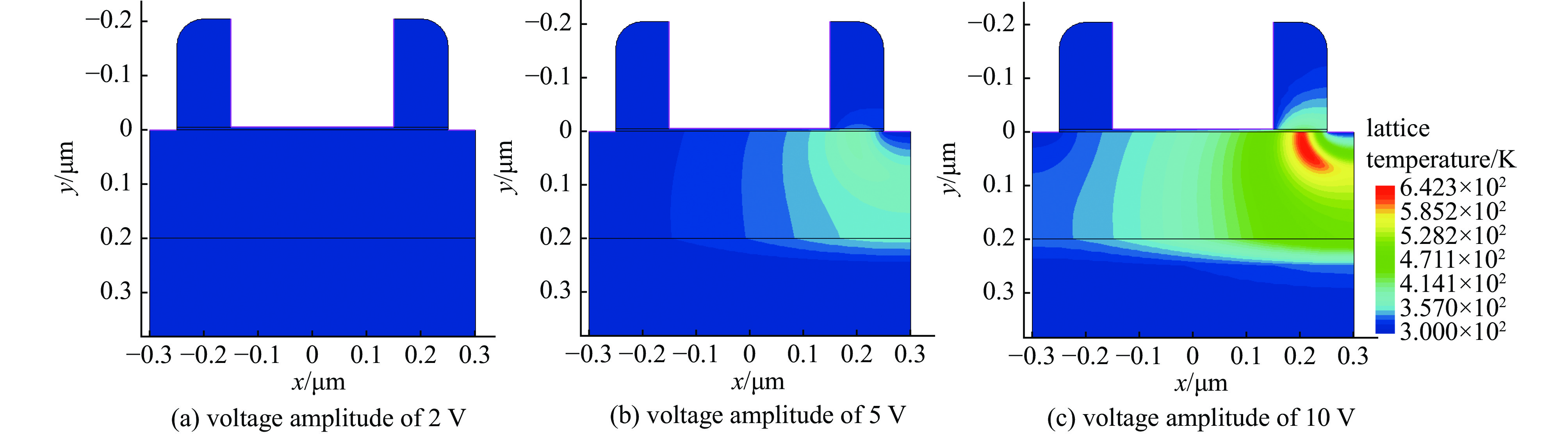
图 9 脉冲电压幅值分别为2 V、5 V和10 V时器件内部温度分布
Figure 9. Internal temperature distribution of the device at pulse voltage amplitudes of 2 V, 5 V, and 10 V
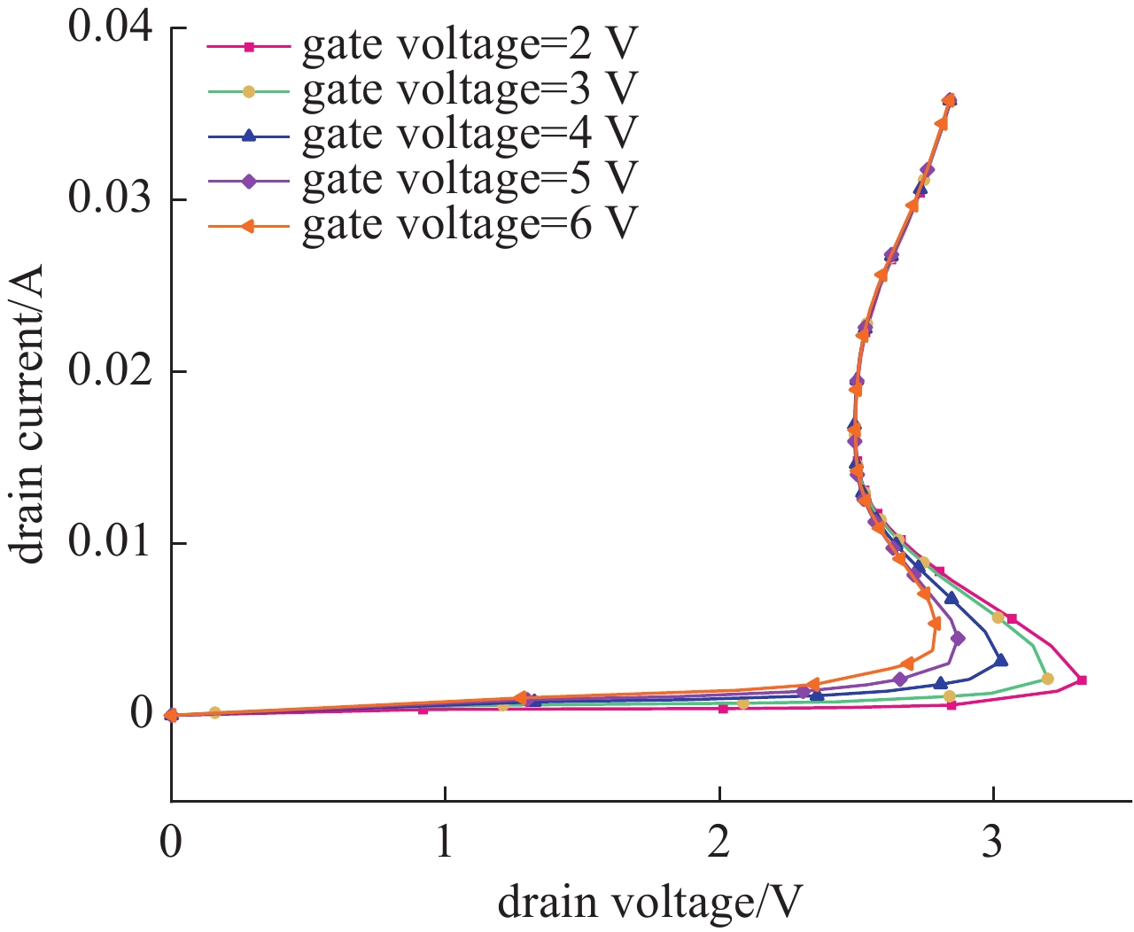
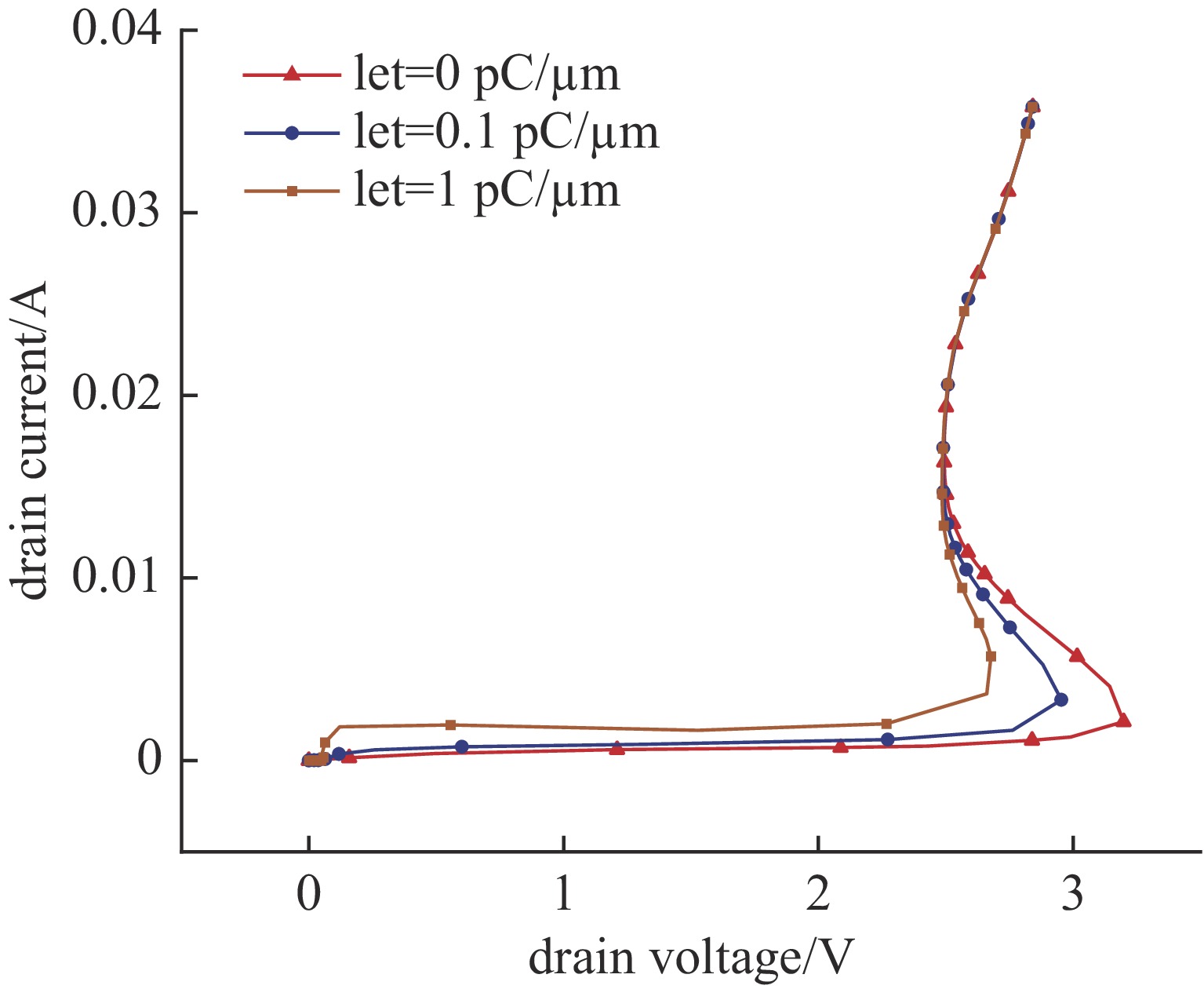
图 10 不同栅极电压下的输出特性曲线
Figure 10. Output characteristic curves under different gate voltages
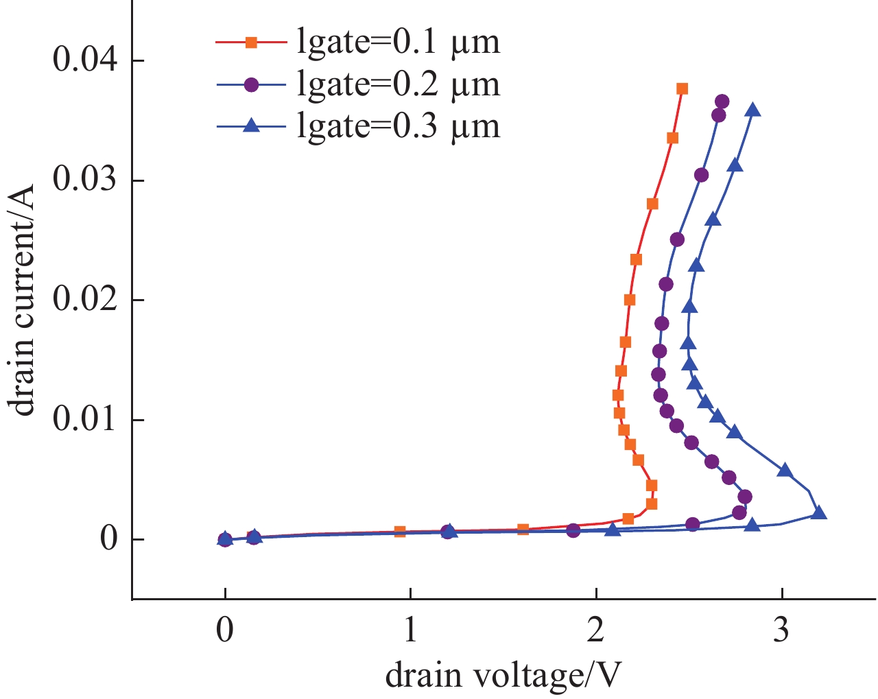
图 11 不同沟道长度下的输出特性曲线
Figure 11. Output characteristic curves at different channel lengths
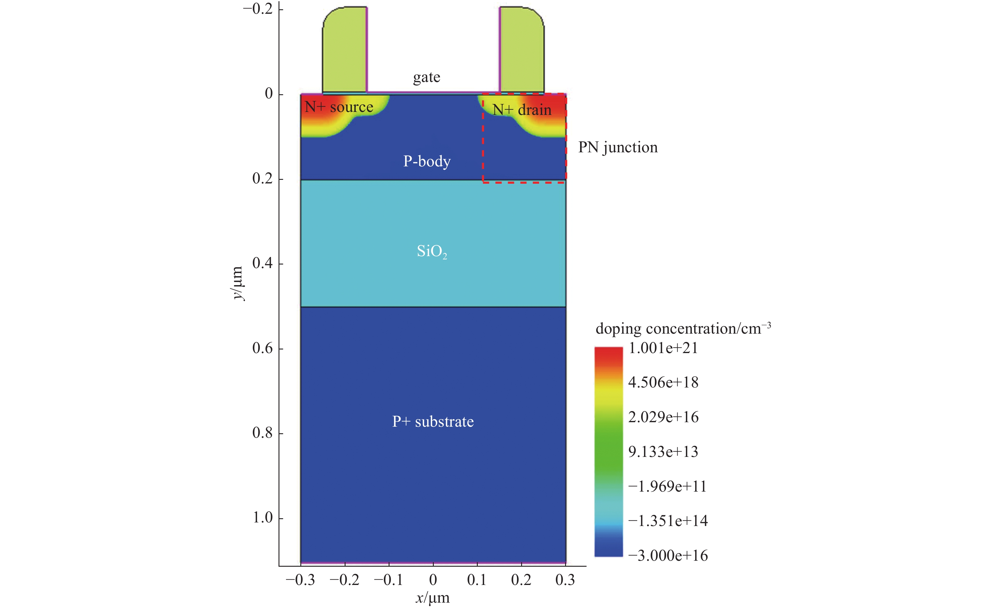
表 1 SOI MOSFET器件结构参数
Table 1. SOI MOSFET device structure parameters
structure thickness/μm material dopant type dopant concentration/cm−3 substrate 0.6 Si B 3×10¹⁵ body 0.2 Si B 3×10¹⁶ drain 0.1 Si P 1×10²¹ source 0.1 Si P 1×10²¹ buried oxide 0.3 SiO2 gate oxide layer 0.003 SiO2 gate 0.2 poly silicon  下载: 导出CSV
-
[1] Doridant A, Jarrix S, Raoult J, et al. Impact of total ionizing dose on the electromagnetic susceptibility of a single bipolar transistor[J]. IEEE Transactions on Nuclear Science, 2012, 59(4): 860-865. doi: 10.1109/TNS.2011.2181415 [2] Lin Jinfu, Liu Hongxia, Wang Shulong, et al. The MOSFET performance degrading induced by electric heating coupling under electromagnetic pulse environment[C]//Proceedings of 2008 IEEE International Conference on Electron Devices and Solid State Circuits (EDSSC). 2018: 1-2. [3] 范菊平, 游海龙, 贾新章. 漏极注入HPM诱发的nMOSFET热电损伤机理[J]. 西北大学学报(自然科学版), 2013, 43(5):724-728Fan Juping, You Hailong, Jia Xinzhang. Research on thermoelectric injury mechanism of nMOSFET due to high power microwave injected from drain[J]. Journal of Northwest University (Natural Science Edition), 2013, 43(5): 724-728 [4] 李万银, 张晨阳, 查继鹏, 等. 电磁脉冲作用下NMOS管的电磁敏感性研究[J]. 兵器装备工程学报, 2023, 44(12):25-31 doi: 10.11809/bqzbgcxb2023.12.004Li Wanyin, Zhang Chenyang, Zha Jipeng, et al. Electromagnetic sensitivity study of NMOS tube under the action of electromagnetic pulse[J]. Journal of Ordnance Equipment Engineering, 2023, 44(12): 25-31 doi: 10.11809/bqzbgcxb2023.12.004 [5] Toyabe T, Yamaguchi K, Asai S, et al. A numerical model of avalanche breakdown in MOSFET’s[J]. IEEE Transactions on Electron Devices, 1978, 57(7): 825-832. [6] 张鸿, 郭红霞, 顾朝桥, 等. SiC JBS二极管和SiC MOSFET的空间辐照效应及机理[J]. 太赫兹科学与电子信息学报, 2022, 20(9):884-896 doi: 10.11805/TKYDA2021444Zhang Hong, Guo Hongxia, Gu Zhaoqiao, et al. Radiation effects of SiC JBS diodes and SiC MOSFETs[J]. Journal of Terahertz Science and Electronic Information Technology, 2022, 20(9): 884-896 doi: 10.11805/TKYDA2021444 [7] 高婷婷, 王玲, 苏凯, 等. 65 nm n沟MOSFET的重离子辐照径迹效应研究[J]. 电子与封装, 2013, 13(5):27-30 doi: 10.3969/j.issn.1681-1070.2013.05.008Gao Tingting, Wang Ling, Su Kai, et al. Track effects study in the 65 nm n-MOSFET irradiated by heavy ions[J]. Electronics & Packaging, 2013, 13(5): 27-30 doi: 10.3969/j.issn.1681-1070.2013.05.008 [8] Estep N A, Petrosky J C, McClory J W, et al. Electromagnetic interference and ionizing radiation effects on CMOS devices[J]. IEEE Transactions on Plasma Science, 2012, 40(6): 1495-1501. doi: 10.1109/TPS.2012.2193600 [9] Wu Wenbin, Zhou Haijing, Zhou Qianhong, et al. Response of NMOS to combined ionization and EMP environments[C]//Proceedings of 2023 International Applied Computational Electromagnetics Society Symposium (ACES-China). 2023: 1-2. [10] Faynot O, Andrieu F, Weber O, et al. Planar Fully depleted SOI technology: a powerful architecture for the 20 nm node and beyond[C]//Proceedings of 2010 International Electron Devices Meeting. 2010: 3.2. 1-3.2. 4. [11] Li Ke, Hao Jianhong, Zhao Qiang, et al. Research on heavy ion irradiation effects on SOI SRAM[J]. Journal of Instrumentation, 2023, 18: P10004. doi: 10.1088/1748-0221/18/10/P10004 [12] 孙毅. 基于TLP的光电器件和CMOS器件电磁脉冲效应的研究[D]. 西安: 西安电子科技大学, 2022Sun Yi. TLP-based research on electromagnetic pulse effect of optoelectronic devices and CMOS devices[D]. Xi’an: Xidian University, 2022 [13] Chong Chen, Li Xing, Liu Hongxia, et al. Study on electromagnetic pulse damage of 22 nm FDSOI in radiation environment[J]. IEEE Transactions on Device and Materials Reliability, 2024, 24(4): 646-655. doi: 10.1109/TDMR.2024.3485095 [14] Azoui T, Tounsi P, Dorkel J M, et al. Estimation of power MOSFET junction temperature during avalanche mode: Experimental tests and modelling[J]. Microelectronics Reliability, 2013, 59(9/11): 1750-1754. [15] 任兴荣, 柴常春, 马振洋, 等. 基极注入强电磁脉冲对双极晶体管的损伤效应和机理[J]. 物理学报, 2013, 62:068501 doi: 10.7498/aps.62.068501Ren Xingrong, Chai Changchun, Ma Zhenyang, et al. The damage effect and mechanism of bipolar transistors induced by injection of electromagnetic pulse from the base[J]. Acta Physica Sinica, 2013, 62: 068501 doi: 10.7498/aps.62.068501 [16] 李嘉骏, 郝敏如. 应变Si MOS器件单粒子辐照效应[J/OL]. 电子科技, 1-6 (2025-01-03). https://doi.org/10.16180/j.cnki.issn1007-7820.2026.04.009Li Jiajun, Hao Minru. Radiation effects of strained Si MOS devices[J/OL]. Electronic Science and Technology, 1-6 (2025-01-03). https://doi.org/10.16180/j.cnki.issn1007-7820.2026.04.009. [17] Atkinson N M. Single-event characterization of a 90-nm bulk CMOS digital cell library[D]. Nashville, TN, USA: Vanderbilt University, 2010. [18] Liu S, Boden M, Girdhar D A, et al. Single-event burnout and avalanche characteristics of power DMOSFETs[J]. IEEE Transactions on Nuclear Science, 2006, 53(6): 3379-3385. doi: 10.1109/TNS.2006.884971 [19] Neamen D A. Semiconductor physics and devices[M]. New York: McGraw-Hill 2012: 182. -

 点击查看大图
计量
- 文章访问数: 45
- HTML全文浏览量: 28
- PDF下载量: 2
- 被引次数: 0
