

Study on GaN-based semiconductor devices for radiation-optical conversion detection
-
摘要: 氮化镓(GaN)材料具有优异的光电性能,可以兼顾半导体和闪烁体的工作模式,在辐射探测领域有广泛的应用潜力。制备了一种由高阻氮化镓衬底层和同质外延多量子阱层串联组合的转换器件,实现了高能辐射在高阻衬底部分激发的载流子通过电场输运至多量子阱实现复合发光。实验表明,器件在工作模式下具有低的暗电流和对X射线灵敏的电学响应。在电场作用下,器件中多量子阱结构发光峰位于410 nm。发光强度随X射线剂量变化有明显提升。通过采集器件发光图像的方法直观验证了器件实现辐射到光信号的转换功能。Abstract:
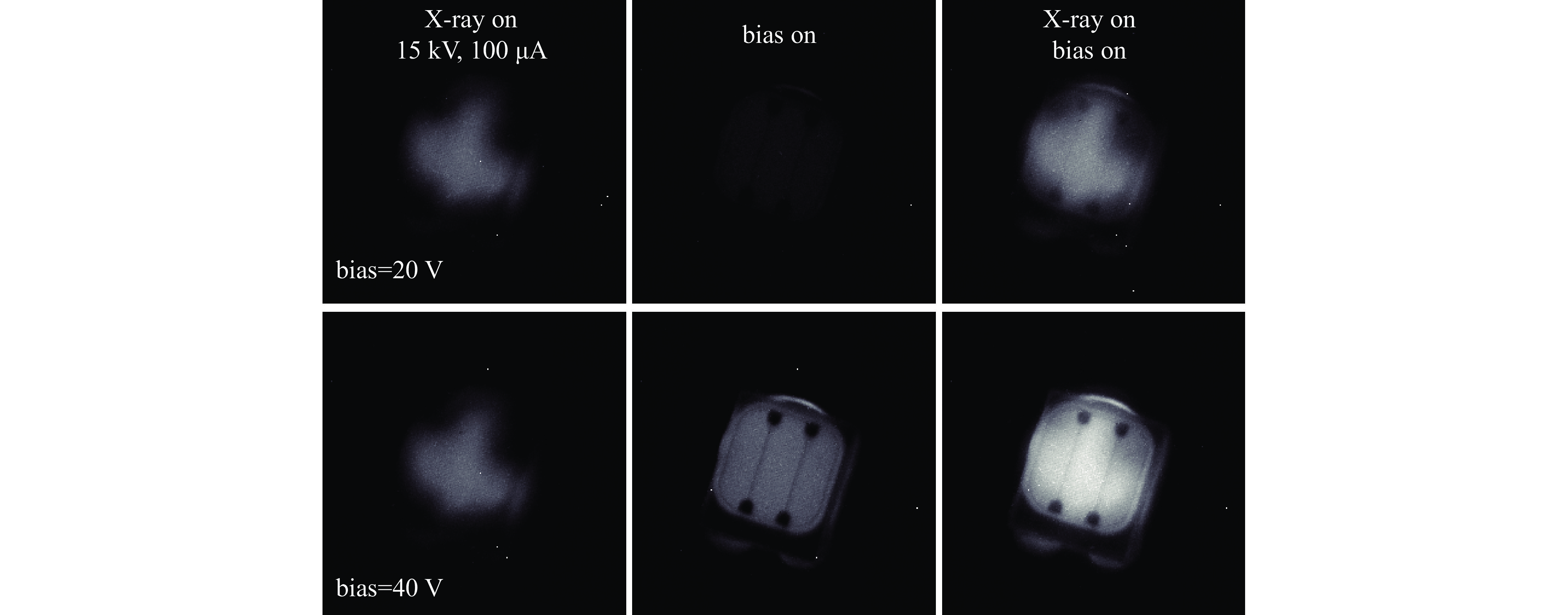
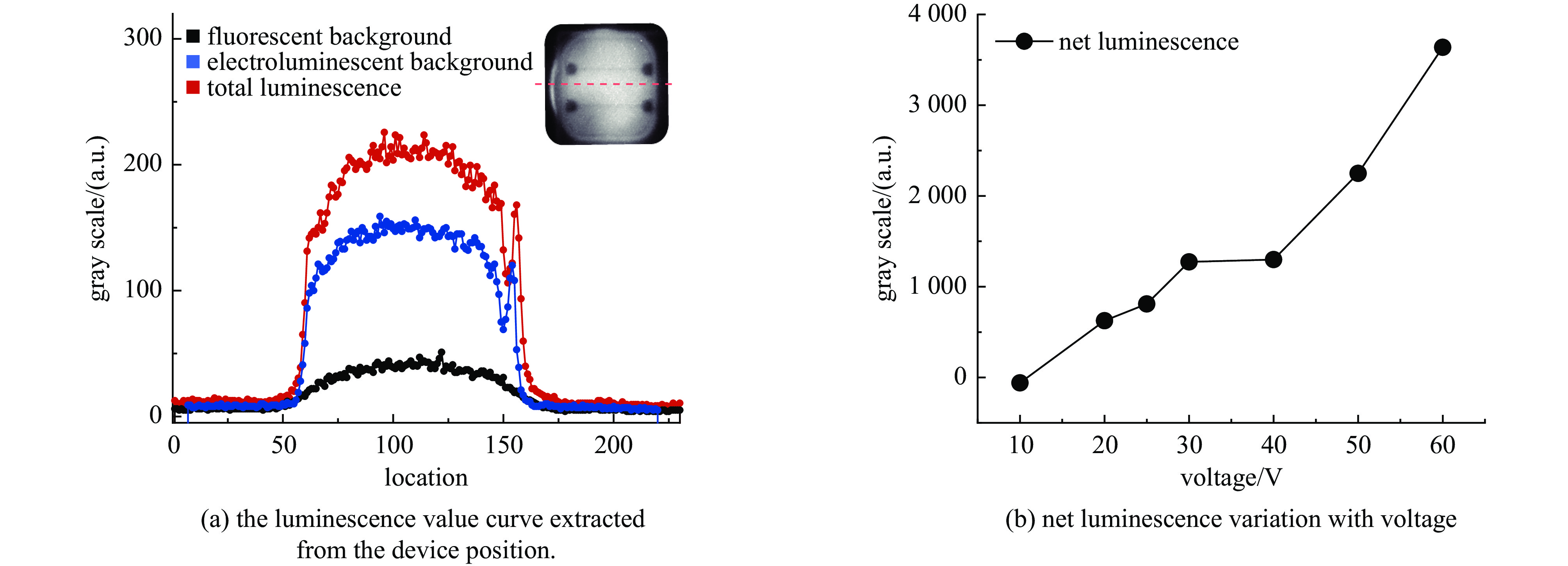
Background Gallium nitride (GaN) exhibits exceptional optoelectronic properties, making it highly suitable for applications in high-power devices, light-emitting diodes (LEDs), high-electron-mobility transistors (HEMTs), and radiation detectors. Particularly in radiation detection, GaN can function as both a semiconductor and a scintillator. As a scintillator material, it demonstrates high luminescence efficiency. However, the yellow luminescence band induced by defects in the material often leads to slow time response, limiting its broader application. On the other hand, GaN-based LEDs with multi-quantum well (MQW) structures can achieve excellent electroluminescence performance. Nevertheless, MQW-enhanced scintillators generally suffer from drawbacks such as a thin sensitive layer and low energy deposition efficiency.Purpose To leverage the advantageous properties of GaN comprehensively and achieve higher overall performance in detection, this study proposes a radiation-to-optical conversion detection mode that combines GaN semiconductor devices for simultaneous radiation energy deposition and carrier recombination luminescence. By constructing a PN junction structure incorporating MQWs on a high-resistivity, high-mobility GaN substrate, a radiation detection device capable of both radiation-to-carrier conversion and carrier recombination luminescence is realized.Methods A 400 μm-thick unintentionally doped high-resistivity GaN single crystal was used as the radiation energy deposition layer. A PN junction structure with MQWs was epitaxially grown on the high-resistivity GaN substrate via metal-organic chemical vapor deposition (MOCVD). The epitaxial layer was segmented into independent regions using inductively coupled plasma (ICP) etching. Transparent indium tin oxide (ITO) electrodes were subsequently fabricated via magnetron sputtering, followed by the deposition of metal electrodes on both the top and bottom surfaces of the device.Results The device exhibited low dark current and sensitive X-ray response characteristics. A multi-quantum well recombination structure with a luminescence peak at 410 nm was incorporated into the device. Luminescence spectrum tests and imaging analysis confirmed the device’s response to varying radiation doses and changes in luminescence efficiency under different applied voltages.Conclusions The designed device enables directional drift and recombination luminescence of carriers generated by radiation energy deposition under an applied electric field. By leveraging semiconductor device design and electric-field-regulated carrier behavior, the luminescence efficiency, response time, and emission spectrum of the device can be effectively modulated. This approach offers a novel technical pathway for radiation detection. -
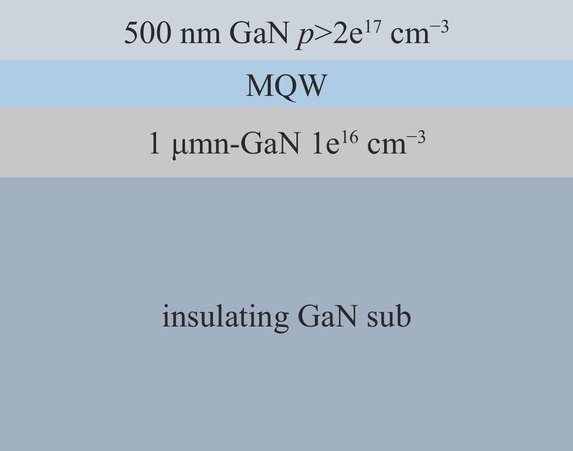
图 2 GaN基射线-光转换器件结构示意图
Figure 2. Schematic diagram of GaN-based radiation-optical conversion device
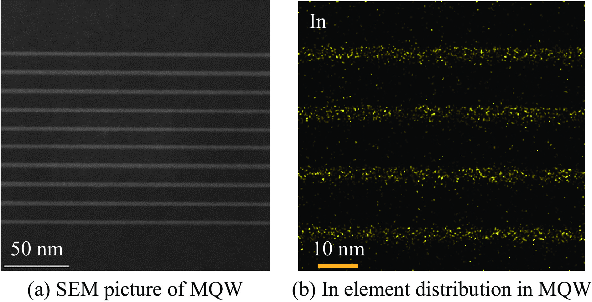
图 3 多量子阱结构扫描电镜照片及EDS面扫图像
Figure 3. Scanning electron micrograph of multi-quantum well structure and EDS surface scanning image
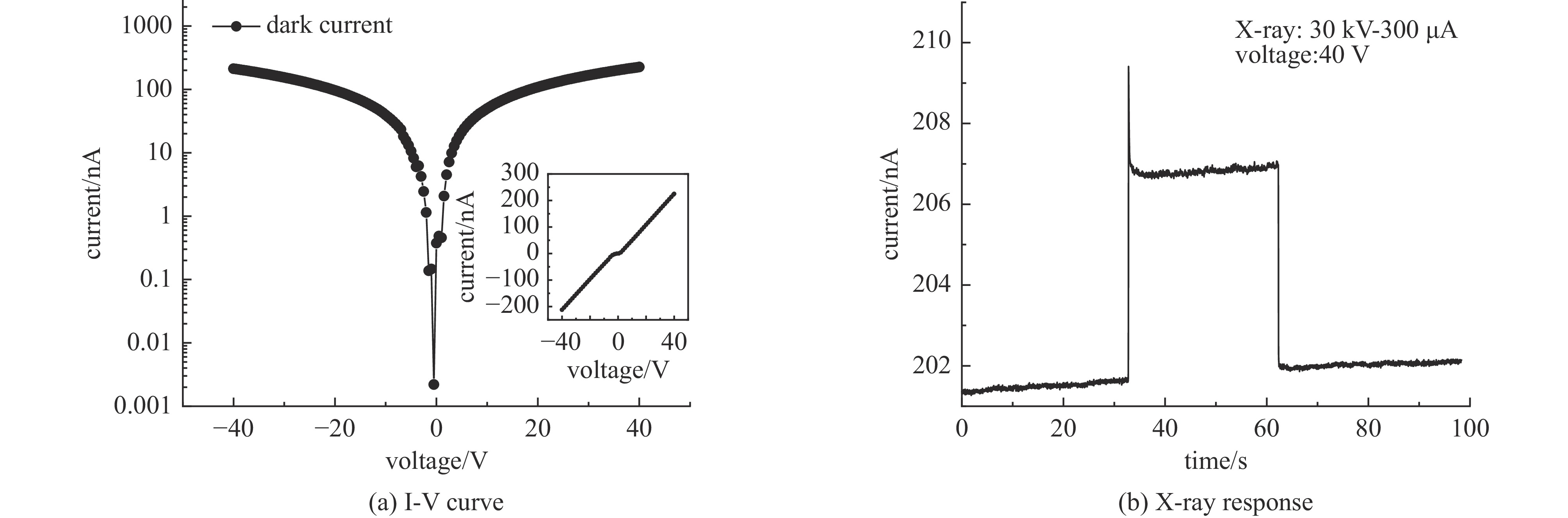
图 4 器件的暗电流I-V曲线和X射线响应曲线
Figure 4. Dark current I-V curve and X-ray response curve of the device
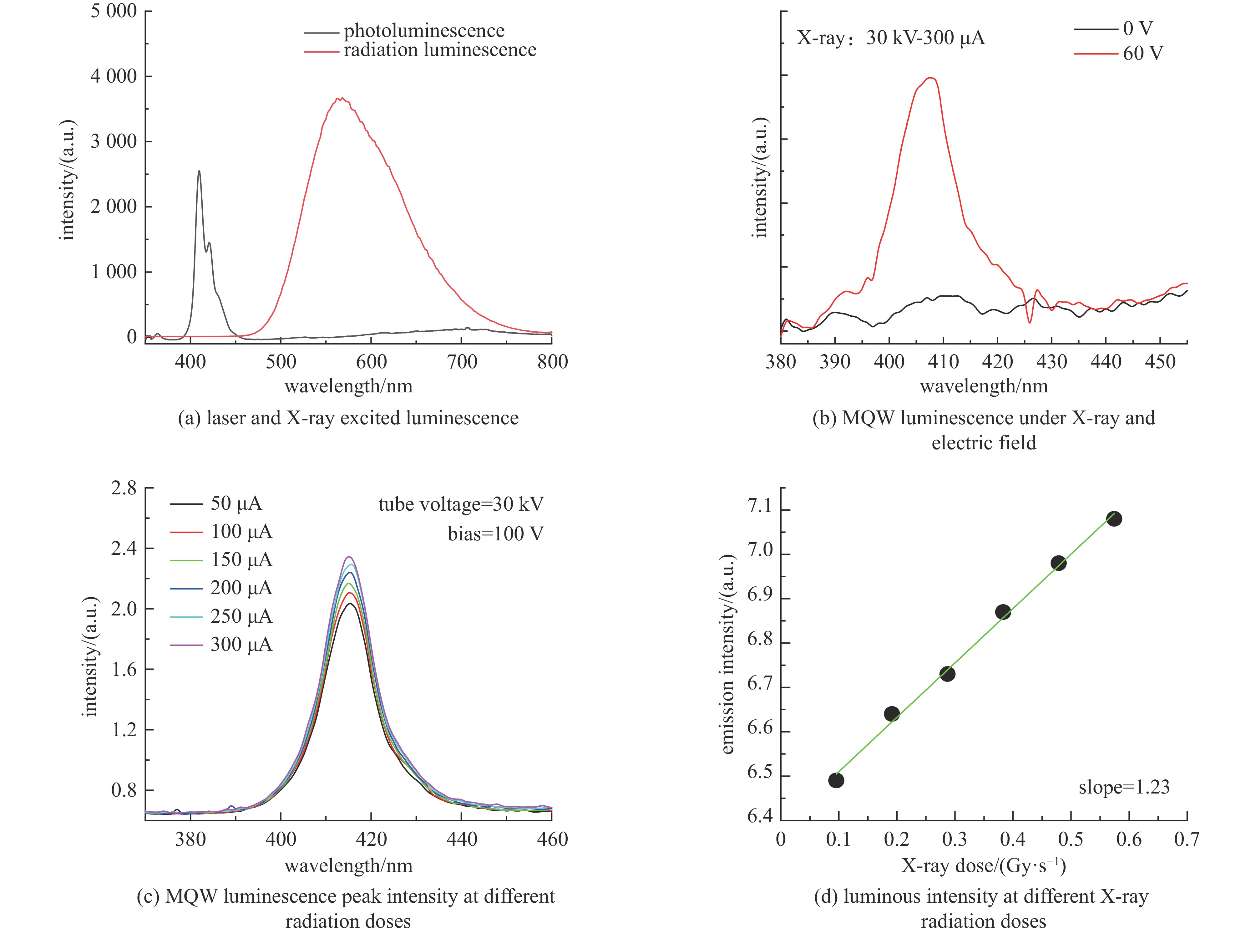
图 5 器件在激光、X射线及电场作用下的发光光谱
Figure 5. Photoluminescence spectra of devices under the action of laser, X-ray and electric field
-
[1] 刘洋, 苏春磊, 欧阳晓平, 等. 电流型GaN辐射探测器研制[J]. 现代应用物理, 2013, 4(4): 319-322 doi: 10.3969/j.issn.2095-6223.2013.04.003Liu Yang, Su Chunlei, Ouyang Xiaoping, et al. A current mode GaN radiation detector[J]. Modern Applied Physics, 2013, 4(4): 319-322 doi: 10.3969/j.issn.2095-6223.2013.04.003 [2] Pearton S J, Zolper J C, Shul R J, et al. GaN: processing, defects, and devices[J]. Journal of Applied Physics, 1999, 86(1): 1-78. doi: 10.1063/1.371145 [3] Gao Hengjie. Advancements and future prospects of Gallium Nitride (GaN) in semiconductor technology[J]. Applied and Computational Engineering, 2024, 65(1): 37-44. doi: 10.54254/2755-2721/65/20240468 [4] 梁勤金, 陈世韬, 余川, 等. 1.2kW C波段固态高效率GaN微波源研制[J]. 强激光与粒子束, 2014, 26: 103002 doi: 10.3788/HPLPB20142610.103002Liang Qinjin, Chen Shitao, Yu Chuan, et al. Development of 1.2kW C band solid-state high efficiency GaN microwave source[J]. High Power Laser and Particle Beams, 2014, 26: 103002 doi: 10.3788/HPLPB20142610.103002 [5] Yao Yuxuan, Liang Yue, Guo Jiabao, et al. The development and applications of nanoporous gallium nitride in optoelectronics: a review[J]. Semiconductor Science and Technology, 2023, 38: 074001. doi: 10.1088/1361-6641/accd14 [6] 邱一武, 董磊, 殷亚楠, 等. 共源共栅结构GaN HEMT器件高能质子辐射效应[J]. 强激光与粒子束, 2025, 37: 024003 doi: 10.11884/HPLPB202537.240223Qiu Yiwu, Dong Lei, Yin Yanan, et al. High-energy proton irradiation effect of Cascode structure GaN HEMT device[J]. High Power Laser and Particle Beams, 2025, 37: 024003 doi: 10.11884/HPLPB202537.240223 [7] Kumar A S, Dalcanale S, Uren M J, et al. Gallium nitride multichannel devices with latch-induced sub-60-mV-per-decade subthreshold slopes for radiofrequency applications[J]. Nature Electronics, 2025, 8(6): 510-517. doi: 10.1038/s41928-025-01391-5 [8] 陈泉佑, 赵景涛, 朱小锋, 等. AlGaN/GaN HEMTs器件中子辐照效应实验和数值模拟研究[J]. 现代应用物理, 2023, 14: 010604 doi: 10.12061/j.issn.2095-6223.2023.010604Chen Quanyou, Zhao Jingtao, Zhu Xiaofeng, et al. Experimental study and numerical simulation of neutron irradiation effects on AlGaN/GaN HEMTs[J]. Modern Applied Physics, 2023, 14: 010604 doi: 10.12061/j.issn.2095-6223.2023.010604 [9] 张翱, 孙世峰, 张翔铭, 等. 双端读出提高快中子探测器时间分辨率方法的研究[J]. 现代应用物理, 2024, 15: 050201Zhang Ao, Sun Shifeng, Zhang Xiangming, et al. Temporal resolution optimization of fast neutron detector using dual-ended readout method[J]. Modern Applied Physics, 2024, 15: 050201 [10] 刘金良, 何世熠, 张显鹏, 等. 反冲质子卡阈中子探测靶室偏转磁场设计[J]. 现代应用物理, 2023, 14: 010204 doi: 10.12061/j.issn.2095-6223.2023.010204Liu Jinliang, He Shiyi, Zhang Xianpeng, et al. Deflecting magnetic field design for recoil-proton neutron detection system with high energy threshold[J]. Modern Applied Physics, 2023, 14: 010204 doi: 10.12061/j.issn.2095-6223.2023.010204 [11] 朱伟龙, 王鹏, 郑辰雅, 等. 基于GaN的高频高功率密度混合集成电源设计[J]. 强激光与粒子束, 2025, 37: 035015 doi: 10.11884/HPLPB202537.240318Zhu Weilong, Wang Peng, Zheng Chenya, et al. Design of high-frequency, high-power density hybrid integrated power supply based on GaN high electron mobility transistors[J]. High Power Laser and Particle Beams, 2025, 37: 035015 doi: 10.11884/HPLPB202537.240318 [12] Chen Lu. Design and application of high-efficiency gallium nitride (GaN)-based power electronic devices[J]. Applied and Computational Engineering, 2025, 153(1): 90-95. doi: 10.54254/2755-2721/2025.23350 [13] Xiong Yixin, Sadek M, Chu Rongming. Recent advances in GaN-based power devices and integration[J]. Semiconductor Science and Technology, 2025, 40: 033002. doi: 10.1088/1361-6641/adb32d [14] Fan Yutong, Liu Xi, Zhang Weihang, et al. Monolithic heterogeneous integration of Si(100)/GaN CMOS inverters and normally-off GaN power devices for high switching frequency and high power applications[C]//2024 36th International Symposium on Power Semiconductor Devices and ICs (ISPSD). 2024: 267-270. [15] 王馨梅, 郑泽彬, 范樱宝, 等. 基于等离子体紫外辐射的强激光自动寻焦系统[J]. 强激光与粒子束, 2019, 31: 091006 doi: 10.11884/HPLPB201931.190252Wang Xinmei, Zheng Zebin, Fan Yingbao, et al. A focus automatic positioning system of high-power laser beam based on plasma ultraviolet radiation[J]. High Power Laser and Particle Beams, 2019, 31: 091006 doi: 10.11884/HPLPB201931.190252 [16] Wakui M, Hu Fangren, Sameshima H, et al. Growth of GaN LED structure on Si substrate by MBE and monolithic fabrication of GaN LED cooling system[J]. IEEJ Transactions on Electrical and Electronic Engineering, 2010, 5(2): 171-174. doi: 10.1002/tee.20513 [17] Huang H W, Kao C C, Chu J T, et al. Investigation of GaN LED with Be-implanted Mg-doped GaN layer[J]. Materials Science and Engineering: B, 2004, 113(1): 19-23. doi: 10.1016/j.mseb.2004.05.024 [18] Jin Xiaomin, Trieu S, Chavoor G J, et al. Enhancing GaN LED efficiency through nano-gratings and standing wave analysis[J]. Nanomaterials, 2018, 8: 1045. doi: 10.3390/nano8121045 [19] Pittet P, Lu Guoneng, Galvan J M, et al. Implantable real-time dosimetric probe using GaN as scintillation material[J]. Sensors and Actuators A: Physical, 2009, 151(1): 29-34. doi: 10.1016/j.sna.2009.02.018 [20] Schenk H P D, Borenstain S I, Berezin A, et al. Cathodoluminescence of epitaxial GaN and ZnO thin films for scintillator applications[J]. Journal of Crystal Growth, 2009, 311(16): 3984-3988. doi: 10.1016/j.jcrysgro.2009.06.018 [21] Li Qiubo, Liu Guangxia, Wang Shouzhi, et al. The effect of GaN single crystal substrate characteristics on homo-epitaxial GaN films[J]. Surfaces and Interfaces, 2025, 56: 105554. doi: 10.1016/j.surfin.2024.105554 [22] Toci G, Gizzi L A, Koester P, et al. InGaN/GaN multiple quantum well for superfast scintillation application: photoluminescence measurements of the picosecond rise time and excitation density effect[J]. Journal of Luminescence, 2019, 208: 119-124. doi: 10.1016/j.jlumin.2018.12.034 [23] Hoffmann A, Holst J, Kaschner A, et al. Impact of the ZnO buffer on the optical properties of GaN: time resolved micro-photoluminescence[J]. Materials Science and Engineering: B, 1999, 59(1/3): 163-167. [24] Demchenko D O, Diallo I C, Reshchikov M A. Yellow luminescence of gallium nitride generated by carbon defect complexes[J]. Physical Review Letters, 2013, 110: 087404. doi: 10.1103/PhysRevLett.110.087404 [25] Stoddard N, Pimputkar S. Progress in ammonothermal crystal growth of gallium nitride from 2017-2023: process, defects and devices[J]. Crystals, 2023, 13: 1004. doi: 10.3390/cryst13071004 [26] Jin S R, Ramsteiner M, Grahn H T, et al. Suppression of yellow luminescence in As-doped GaN epilayers grown by metalorganic chemical vapor deposition[J]. Journal of Crystal Growth, 2000, 212(1/2): 56-60. [27] Rodrigues J, Miranda S M C, Fernandes A J S, et al. Towards the understanding of the intentionally induced yellow luminescence in GaN nanowires[J]. Physica Status Solidi C, 2013, 10(4): 667-672. doi: 10.1002/pssc.201200714 [28] Hsu Y P, Chang S J, Su Y K, et al. InGaN–GaN MQW LEDs with Si treatment[J]. IEEE Photonics Technology Letters, 2005, 17(8): 1620-1622. doi: 10.1109/LPT.2005.851989 [29] Ferdous M S, Wang X, Fairchild M N, et al. Effect of threading defects on InGaN/GaN multiple quantum well light emitting diodes[J]. Applied Physics Letters, 2007, 91: 231107. doi: 10.1063/1.2822395 [30] Hospodková A, Nikl M, Pacherová O, et al. InGaN/GaN multiple quantum well for fast scintillation application: radioluminescence and photoluminescence study[J]. Nanotechnology, 2014, 25: 455501. doi: 10.1088/0957-4484/25/45/455501 [31] 陈志忠, 徐科, 秦志新, 等. InGaN/GaN多量子阱LED电致发光谱中双峰起源的研究[J]. 半导体学报, 2007, 28(7): 1121-1124Chen Zhizhong, Xu Ke, Qin Zhixin, et al. Origins of double emission peaks in electroluminescence spectrum from InGaN/GaN MQW LED[J]. Chinese Journal of Semiconductors, 2007, 28(7): 1121-1124 [32] O’Donovan M, Farrell P, Moatti J, et al. Impact of random alloy fluctuations on the carrier distribution in multi-color (In, Ga)N/GaN quantum well systems[J]. Physical Review Applied, 2024, 21: 024052. doi: 10.1103/PhysRevApplied.21.024052 -

 下载:
下载:
 点击查看大图

计量
- 文章访问数: 110
- HTML全文浏览量: 25
- PDF下载量: 9
- 被引次数: 0
