

Applications of neutron diffraction in semiconductor materials and devices research
-
摘要: 中子衍射技术凭借其穿透能力、轻元素敏感性和动态探测优势,成为半导体材料研究的重要表征手段。该技术通过分析衍射峰特征,揭示材料的晶格畸变、应变分布和缺陷演化规律,为理解材料性能提供原子尺度依据。它能定量分析位错密度和阳离子占位等缺陷,并研究磁有序结构和自旋相互作用机制,支撑新型电子器件开发。其原位测试能力可实时观测相变过程中的缺陷重组动态,揭示外场作用下的结构响应机制,尤其在极端环境材料研究中克服了传统方法的局限。当前研究重点转向建立微观结构与宏观性能的关联模型,发展原位动态测试方法以精准预测材料行为。随着大型科学装置的升级,该技术将在半导体材料的基础研究和工程应用中发挥更大作用,特别是在苛刻环境材料开发领域前景广阔。未来发展方向将聚焦多尺度表征能力提升和原位实验方法创新,为半导体材料科学进步提供有力支撑。Abstract: Neutron diffraction technology has become a vital characterization tool in semiconductor material research due to its penetration capability, sensitivity to light elements, and dynamic detection advantages. By analyzing diffraction peak characteristics, this technique reveals lattice distortions, strain distributions, and defect evolution patterns, providing atomic-scale insights into material properties. It enables quantitative analysis of defects such as dislocation density and cation occupancy while investigating magnetic ordering and spin interaction mechanisms, supporting the development of novel electronic devices. Its in-situ testing capability allows real-time observation of defect reorganization during phase transitions and structural responses under external fields, overcoming the limitations of conventional methods, particularly in extreme-environment material studies. Current research focuses on establishing correlations between microstructural evolution and macroscopic performance, advancing in-situ dynamic testing methods for precise material behavior prediction. With upgrades to large-scale scientific facilities, neutron diffraction will play an increasingly significant role in both fundamental research and engineering applications of semiconductor materials, especially in harsh-environment material development. Future advancements will prioritize enhancing multiscale characterization capabilities and innovating in-situ experimental approaches, providing robust technical support for semiconductor materials science.
-
Key words:
- radiation damage /
- neutron diffraction /
- semiconductor devices /
- microstructure /
- extreme conditions
-
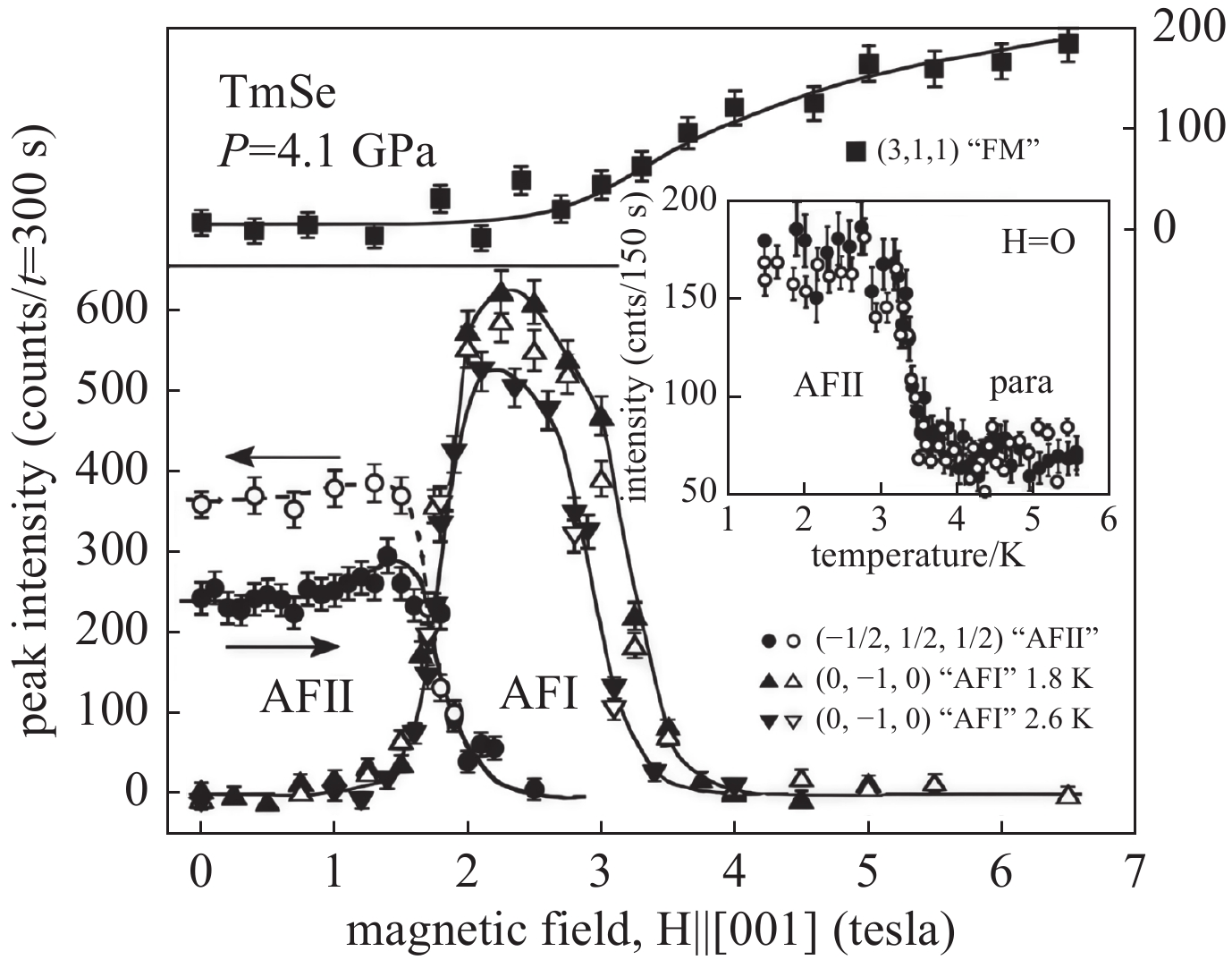
图 4 沿[001]晶轴方向施加磁场H的条件下,与铁磁相(上图)、AF I相及AF II相(下图)波矢相关的磁衍射峰强度,测量温度范围为1.5~1.8 K。插图显示了零场条件下(-
$ \dfrac{1}{2} $ ,$ \dfrac{1}{2} $ ,$ \dfrac{1}{2} $ )峰强度随温度的变化[24]Figure 4. Under an applied magnetic field H along the [001] crystallographic axis, the intensities of magnetic diffraction peaks associated with the wave vectors of the ferromagnetic phase (upper panel), AF I phase and AF II phase (lower panel) were measured in the temperature range of 1.5~1.8 K. The inset shows the temperature dependence of the (−1/2,1/2,1/2) peak intensity under zero-field conditions[24]
-
[1] Woracek R, Santisteban J, Fedrigo A, et al. Diffraction in neutron imaging—A review[J]. Nuclear Instruments and Methods in Physics Research Section A: Accelerators, Spectrometers, Detectors and Associated Equipment, 2018, 878: 141-158. [2] 林皓, 李建, 杨钊龙, 等. 中子衍射应力分析技术及其应用进展[J]. 金属学报, 2024, 60(8): 1017-1030 doi: 10.11900/0412.1961.2024.00061Lin Hao, Li Jian, Yang Zhaolong, et al. Recent progress in stress analysis technology and application of neutron diffraction[J]. Acta Metallurgica Sinica, 2024, 60(8): 1017-1030 doi: 10.11900/0412.1961.2024.00061 [3] 郑海彪, 康乐, 陈洁, 等. 多场耦合原位拉伸中子衍射实验装置综述[J]. 强激光与粒子束, 2024, 36: 106002 doi: 10.11884/HPLPB202436.240207Zheng Haibiao, Kang Le, Chen Jie, et al. A review of multi-field coupled in-situ stretching neutron diffraction experimental devices[J]. High Power Laser and Particle Beams, 2024, 36: 106002 doi: 10.11884/HPLPB202436.240207 [4] 王立鹏, 孔令体, 姜夺玉, 等. 基于经典分子动力学模拟的热中子散射数据产生方法[J]. 现代应用物理, 2025, 16: 020203 doi: 10.12061/j.issn.2095-6223.202407039Wang Lipeng, Kong Lingti, Jiang Duoyu, et al. Thermal neutron scattering data generation method based on classical molecular dynamics simulations[J]. Modern Applied Physics, 2025, 16: 020203 doi: 10.12061/j.issn.2095-6223.202407039 [5] Roehrens D, Brendt J, Samuelis D, et al. On the ammonolysis of Ga2O3: an XRD, neutron diffraction and XAS investigation of the oxygen-rich part of the system Ga2O3–GaN[J]. Journal of Solid State Chemistry, 2010, 183(3): 532-541. doi: 10.1016/j.jssc.2009.12.024 [6] Suehiro T, Tansho M, Hagihala M, et al. Quaternary nitride system (1−x)ZnGeN2−2xGaN (x = 1/3): disordered wurtzite structure revealed by time-of-flight neutron powder diffraction[J]. Applied Physics Express, 2020, 13: 115503. doi: 10.35848/1882-0786/abc1cb [7] Dong Liran, Zhang Jie, Li Yizhuang, et al. Borrowed dislocations for ductility in ceramics[J]. Science, 2024, 385(6707): 422-427. doi: 10.1126/science.adp0559 [8] Dhanalakshmi Veeraraj M R, Qu Di, Zhao Shuai, et al. Diffractive lenses for neutron techniques[J]. Scientific Reports, 2025, 15: 8408. doi: 10.1038/s41598-025-92329-6 [9] Martel P, Rogers D, Stephens A E. Neutron diffraction as a rapid screening method for semiconductor wafers[J]. Applied Physics Letters, 1987, 51(22): 1795-1797. doi: 10.1063/1.98525 [10] 谭志新, 敬罕涛, 樊瑞睿, 等. 中国散裂中子源伴生质子辐照实验平台及其技术参数的确定[J]. 现代应用物理, 2024, 15: 020401 doi: 10.12061/j.issn.2095-6223.2024.020401Tan Zhixin, Jing Hantao, Fan Ruirui, et al. Associated protons experimental platform of China spallation neutron source and determination of its technical parameters[J]. Modern Applied Physics, 2024, 15: 020401 doi: 10.12061/j.issn.2095-6223.2024.020401 [11] Wang Yanxu, Gong Wu, Kawasaki T, et al. In situ neutron diffraction study on the deformation behavior of the plastic inorganic semiconductor Ag2S[J]. Applied Physics Letters, 2023, 123: 011903. doi: 10.1063/5.0158607 [12] Bokuchava G D. Materials microstructure characterization using high resolution time-of-flight neutron diffraction[J]. Romanian Journal of Physics, 2016, 61(5/6): 903-925. [13] Son B S, Kim S J, Lee B W, et al. Mössbauer spectroscopy and neutron diffraction studies of the ferrimagnetic semiconductor on Ga-substituted FeGaxCr2−xS4[J]. Journal of Applied Physics, 2005, 97: 10D322. doi: 10.1063/1.1854051 [14] Wang Zhenyu, Breternitz J, Schorr S. Cation disorder in zinc-group IV- nitride and oxide nitride semiconductor materials revealed through neutron diffraction[J]. Acta Crystallographica Section A: Foundations and Advances, 2021, A77: C1077. [15] Hanada T, Izumi F, Nakamura Y, et al. Neutron and electron diffraction studies of ZnGa2Se4[J]. Physica B: Condensed Matter, 1997, 241/243: 373-375. [16] Rhyne J J, Lin J, Furdyna J K, et al. Anomalous antiferromagnetic coupling in [ZnTe¦MnTe] superlattices[J]. Journal of Magnetism and Magnetic Materials, 1998, 177/181: 1195-1196. [17] Vennix C W H M, Frikkee E, Swagten H J M, et al. Neutron diffraction on the diluted magnetic semiconductor Sn1−xMnxTe[J]. Journal of Applied Physics, 1991, 69(8): 6025-6027. doi: 10.1063/1.347805 [18] Giebultowicz T M, Kepa H, Blinowski J, et al. Neutron diffraction and reflectivity studies of interlayer correlations in magnetic semiconductor superlattices[J]. Physica E: Low-Dimensional Systems and Nanostructures, 2001, 10(1/3): 411-418. [19] Goldman K I, Springholz G, Kepa H, et al. Interlayer correlations in antiferromagnetic semiconductor superlattices EuTe/PbTe[J]. Physica B: Condensed Matter, 1997, 241/243: 710-713. [20] Kȩpa H, Kutner-Pielaszek J, Twardowski A, et al. Interlayer correlations in ferromagnetic semiconductor superlattices EuS/PbS[J]. Journal of Magnetism and Magnetic Materials, 2001, 226/230: 1795-1797. [21] Dolling G, Holden T M, Sears V F, et al. Neutron diffraction studies of diluted magnetic semiconductors (invited)[J]. Journal of Applied Physics, 1982, 53(11): 7644-7648. doi: 10.1063/1.330174 [22] Messenger G C. A summary review of displacement damage from high energy radiation in silicon semiconductors and semiconductor devices[J]. IEEE Transactions on Nuclear Science, 1992, 39(3): 468-473. doi: 10.1109/23.277547 [23] Nikam R, Kurawle N, Borole S, et al. Neutron diffraction studies of Fe-substituted Mn2O3[J]. Indian Journal of Physics, 2023, 97(9): 2721-2725. doi: 10.1007/s12648-023-02621-2 [24] Mignot J M, Goncharenko I N, Matsumura T, et al. Magnetic phase diagram of the mixed-valence semiconductor TmSe under multi-extreme (P, H, T) conditions[J]. Physica B: Condensed Matter, 2005, 359/361: 105-107. [25] Giebultowicz T M, Rhyne J J, Furdyna J K, et al. Neutron diffraction study of the wurtzite-structure dilute magnetic semiconductor Zn0.45Mn0.55Se[J]. Journal of Applied Physics, 1987, 61(8): 3540-3542. doi: 10.1063/1.338717 [26] 熊振鹏. 宽禁带半导体GaN的辐照损伤机理研究[D]. 北京: 华北电力大学(北京), 2023Xiong Zhenpeng. Research on radiation damage mechanism of wide band gap semiconductor GaN[D]. Beijing: North China Electric Power University (Beijing), 2023 [27] 周炜翔, 曹荣幸, 胡迪科, 等. 增强型Cascode结构GaN HEMT器件中子辐照效应研究[J]. 航天器环境工程, 2024, 41(5): 617-624 doi: 10.12126/see.2024010Zhou Weixiang, Cao Rongxing, Hu Dike, et al. Study on neutron irradiation effects of enhancement-mode Cascode-structured GaN HEMT devices[J]. Spacecraft Environment Engineering, 2024, 41(5): 617-624 doi: 10.12126/see.2024010 [28] Zhou Feng, Wang Tianqi, Liu Chaoming, et al. 800-V irradiation-hardened device technology on GaN-on-SiC power integration platform[C]//Proceedings of 2024 IEEE International Electron Devices Meeting. 2024. [29] Berthet F, Guhel Y, Boudart B, et al. Influence of thermal and fast neutron irradiation on dc electrical performances of AlGaN/GaN transistors[J]. IEEE Transactions on Nuclear Science, 2012, 59(5): 2556-2561. doi: 10.1109/TNS.2012.2209894 [30] Brudnyi V N, Boiko V M, Kolin N G, et al. Neutron irradiation-induced modification of electrical and structural properties of GaN epifilms grown on Al2O3 (0001) substrate[J]. Semiconductor Science and Technology, 2018, 33: 095011. doi: 10.1088/1361-6641/aad53b [31] Butler P A, Uren M J, Lambert B, et al. Neutron irradiation impact on AlGaN/GaN HEMT switching transients[J]. IEEE Transactions on Nuclear Science, 2018, 65(12): 2862-2869. doi: 10.1109/TNS.2018.2880287 [32] Gaubas E, Čeponis T, Meškauskaite D, et al. Pulsed photo-ionization spectroscopy of traps in as-grown and neutron irradiated ammonothermally synthesized GaN[J]. Scientific Reports, 2019, 9: 1473. doi: 10.1038/s41598-018-38138-6 [33] Gaubas E, Vaitkus J, Kazlauskas K, et al. Recombination characteristics of the proton and neutron irradiated semi-insulating GaN structures[J]. Nuclear Instruments and Methods in Physics Research Section A: Accelerators, Spectrometers, Detectors and Associated Equipment, 2007, 583(1): 181-184. [34] 谷文萍, 张林, 李清华, 等. 中子辐照对AlGaN/GaN 高电子迁移率晶体管器件电特性的影响[J]. 物理学报, 2014, 63: 047202 doi: 10.7498/aps.63.047202Gu Wenping, Zhang Lin, Li Qinghua, et al. Effect of neutron irradiation on the electrical properties of AlGaN/GaN high electron mobility transistors[J]. Acta Physica Sinica, 2014, 63: 047202 doi: 10.7498/aps.63.047202 [35] 郝蕊静, 郭红霞, 潘霄宇, 等. AlGaN/GaN高电子迁移率晶体管器件中子位移损伤效应及机理[J]. 物理学报, 2020, 69: 207301 doi: 10.7498/aps.69.20200714Hao Ruijing, Guo Hongxia, Pan Xiaoyu, et al. Neutron-induced displacement damage effect and mechanism of AlGaN/GaN high electron mobility transistor[J]. Acta Physica Sinica, 2020, 69: 207301 doi: 10.7498/aps.69.20200714 [36] Kim B J, Kim H Y, Kim J, et al. Neutron irradiation on AlGaN/GaN high electron mobility transistors on SiC substrates[J]. Journal of Crystal Growth, 2011, 326(1): 205-207. doi: 10.1016/j.jcrysgro.2011.01.098 [37] Rajan S, Waltereit P, Poblenz C, et al. Power performance of AlGaN–GaN HEMTs grown on SiC by plasma-assisted MBE[J]. IEEE Electron Device Letters, 2004, 25(5): 247-249. doi: 10.1109/LED.2004.826977 [38] Kyle E C H, Kaun S W, Burke P G, et al. High-electron-mobility GaN grown on free-standing GaN templates by ammonia-based molecular beam epitaxy[J]. Journal of Applied Physics, 2014, 115: 193702. doi: 10.1063/1.4874735 [39] Chen Jin, Puzyrev Y S, Zhang C X, et al. Proton-induced dehydrogenation of defects in AlGaN/GaN HEMTs[J]. IEEE Transactions on Nuclear Science, 2013, 60(6): 4080-4086. doi: 10.1109/TNS.2013.2281771 [40] 郝蕊静. GaN HEMT器件无偏置下中子位移损伤效应研究[D]. 湘潭: 湘潭大学, 2020Hao Ruijing. The effect of neutron induced displacement damage in unbiased GaN HEMT devices[D]. Xiangtan: Xiangtan University, 2020 [41] 邱一武, 马艺珂, 张平威, 等. 增强型AlGaN/GaN HEMT器件中子位移损伤效应研究[J]. 固体电子学研究与进展, 2023, 43(4): 359-365,374Qiu Yiwu, Ma Yike, Zhang Pingwei, et al. Study of neutron induced displacement damage in enhanced AlGaN/GaN HEMT device[J]. Research & Progress of SSE, 2023, 43(4): 359-365,374 [42] Lorenz K, Marques J G, Franco N, et al. Defect studies on fast and thermal neutron irradiated GaN[J]. Nuclear Instruments and Methods in Physics Research Section B: Beam Interactions with Materials and Atoms, 2008, 266(12/13): 2780-2783. [43] Lv Ling, Li Peixian, Ma Xiaohua, et al. Fast and thermal neutron radiation effects on GaN PIN diodes[J]. IEEE Transactions on Nuclear Science, 2017, 64(1): 643-647. doi: 10.1109/TNS.2016.2630061 -

 下载:
下载:


 点击查看大图
图(4)
计量
- 文章访问数: 35
- HTML全文浏览量: 13
- PDF下载量: 2
- 被引次数: 0
