

Simulation and Experimental Investigation of the Channel Electron Multiplier
-
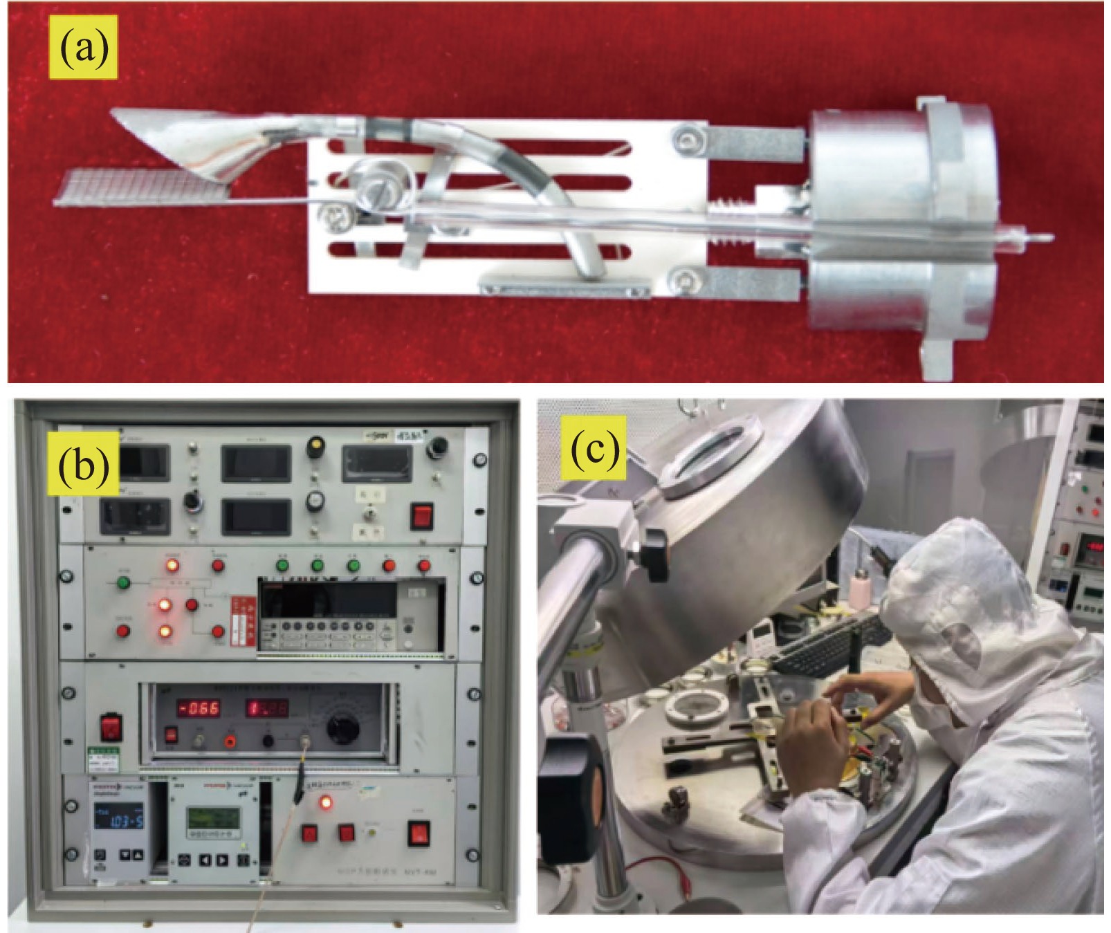
摘要: 单通道电子倍增器(CEM)作为一种高增益电真空器件,广泛应用于质谱分析、空间探测等领域。当前国产CEM普遍存在增益低、一致性较差等问题。从模拟和实验两方面开展了高增益CEM的研制工作。模拟基于CST Studio Suite电子仿真软件,结合有限积分法、Monte Carlo法及Furman二次电子发射模型,构建了CEM三维模型,模拟了电子在CEM通道内的运动轨迹与倍增过程。仿真结果表明:CEM性能与其结构和操作参数以及通道内壁二次电子发射特性相关,当CEM喇叭口直径为13 mm、通道孔径为1.2 mm、通道直桶段长度为14 mm、弯曲段半径为15.5 mm时,CEM增益最高。基于模拟结果,开展了相关实验研究,优化了CEM结构参数。测试结果表明:同等电压下,结构优化后CEM增益提升了近5倍,实验与模拟结果一致。此外,实验采用原子层沉积技术在通道内壁制备了Al2O3膜层,测试结果表明,CEM增益提高了近20倍。为国产CEM的最优结构设计与性能提升提供重要的参考。
-
关键词:
- 单通道电子倍增器 /
- 有限积分法 /
- Monte Carlo法 /
- 原子层沉积 /
- 增益
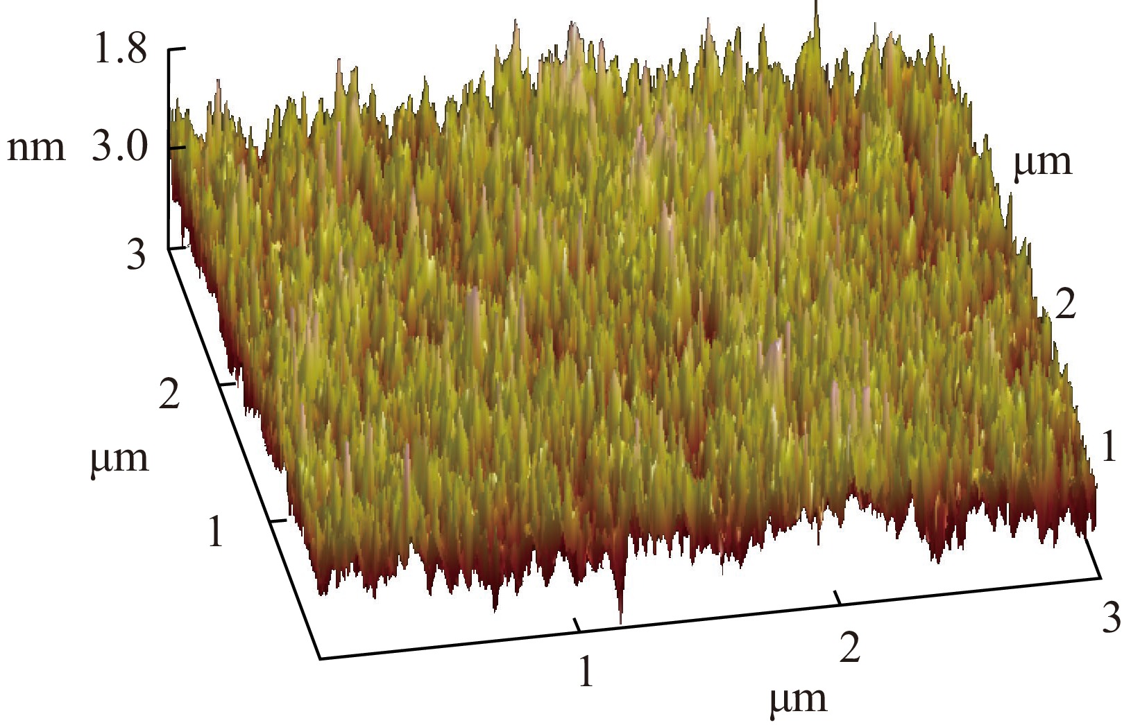
Abstract:Background The Single-Channel Electron Multiplier (CEM), as a high-gain electrovacuum device, is widely utilized in fields such as mass spectrometry and space exploration. Currently, domestically produced CEMs often face challenges including relatively low gain and inconsistent performance.Purpose To address these issues, this study undertakes the development of high-gain CEMs through both simulation and experimental approaches.Methods For the simulation, a three-dimensional model of the CEM was established using CST Studio Suite, incorporating the finite integration technique, the Monte Carlo method, and the Furman secondary electron emission model. This model systematically simulated the electron trajectories and multiplication processes within the channel.Results The simulation results indicate that the electron multiplication characteristics of CEMs are significantly influenced by structural parameters and functional thin films. The optimal structural parameters were identified as a funnel diameter of 13 mm, a channel diameter of 1.2 mm, a straight-channel length of 14 mm, and a bending radius of 15.5 mm.Experimentally, the fabricated CEM channels exhibited consistent morphology with a low film roughness of approximately 0.65 nm, indicating good process consistency and high smoothness of the inner walls, which aligns well with the theoretical design. A comparison between two CEMs with different structural parameters revealed that the optimized structure achieved a nearly fivefold increase in gain under the same operating voltage. Furthermore, after depositing an approximately 5 nm thick Al2O3 functional film on the inner channel wall via atomic layer deposition, the gain of the CEM increased by approximately 20 times under the same voltage, underscoring the critical role of functional films with a high secondary electron emission coefficient in enhancing gain.Conclusions Through theoretical simulation and performance optimization analysis, this study provides key parameter optimization guidelines and a technical foundation for the localized design of CEMs. -
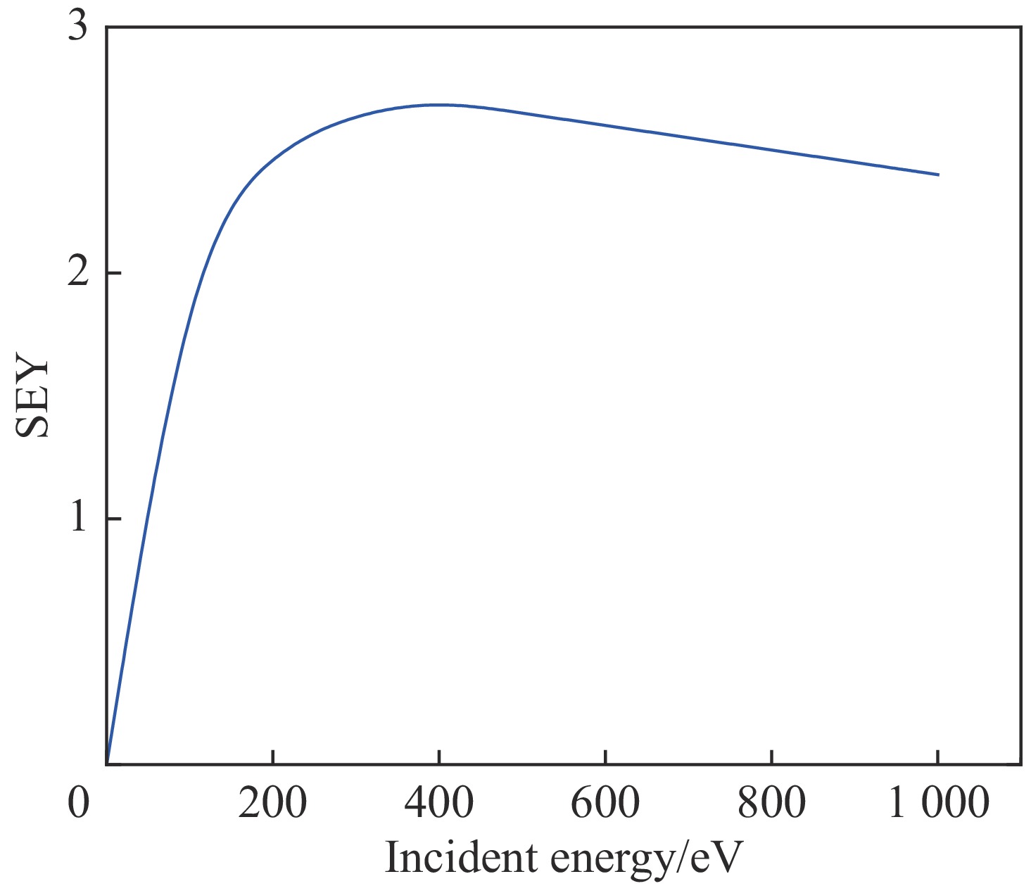
图 2 CEM倍增材料的二次电子发射曲线
Figure 2. Secondary Electron Emission Curve of the CEM Multiplication Material
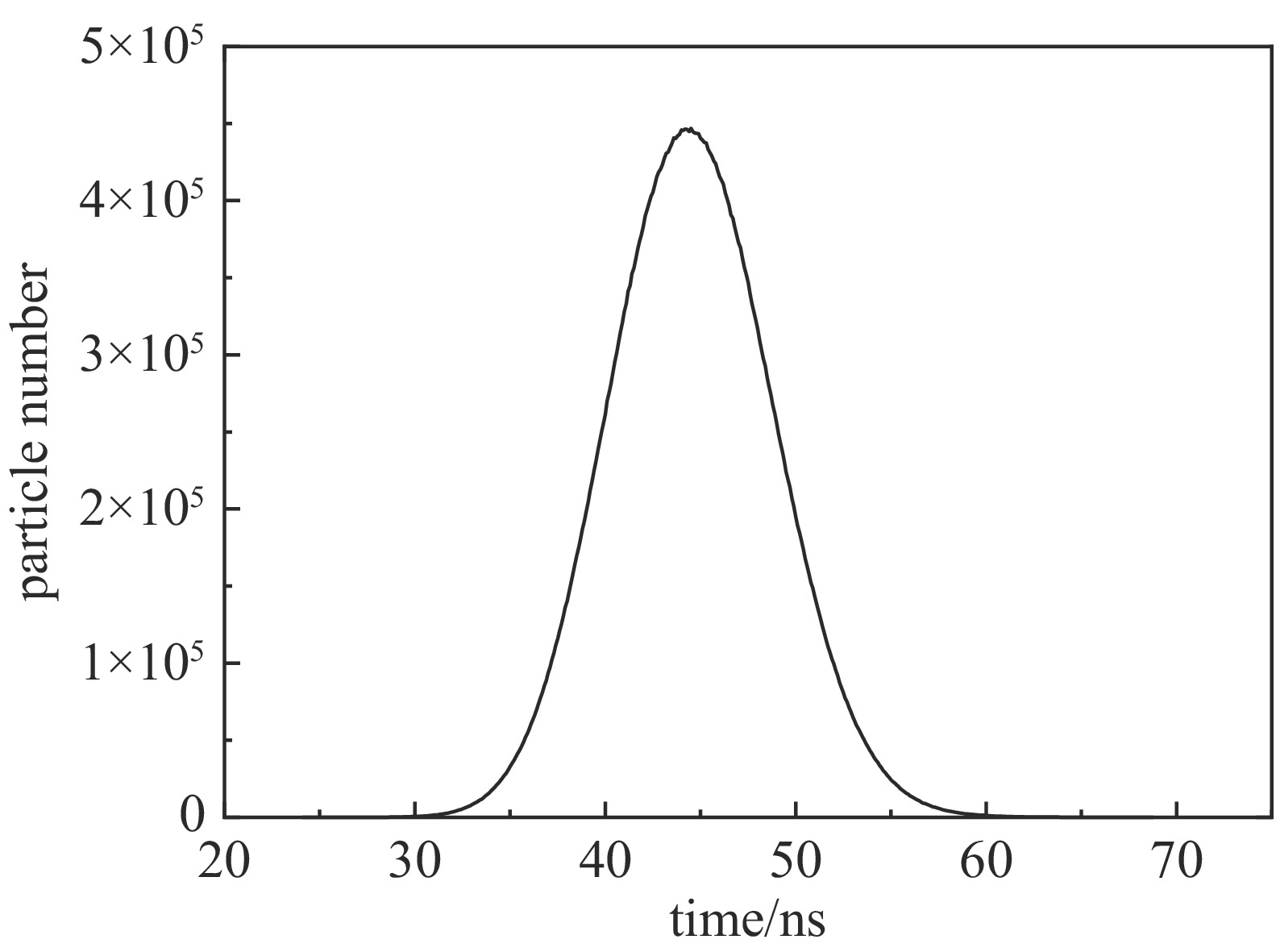
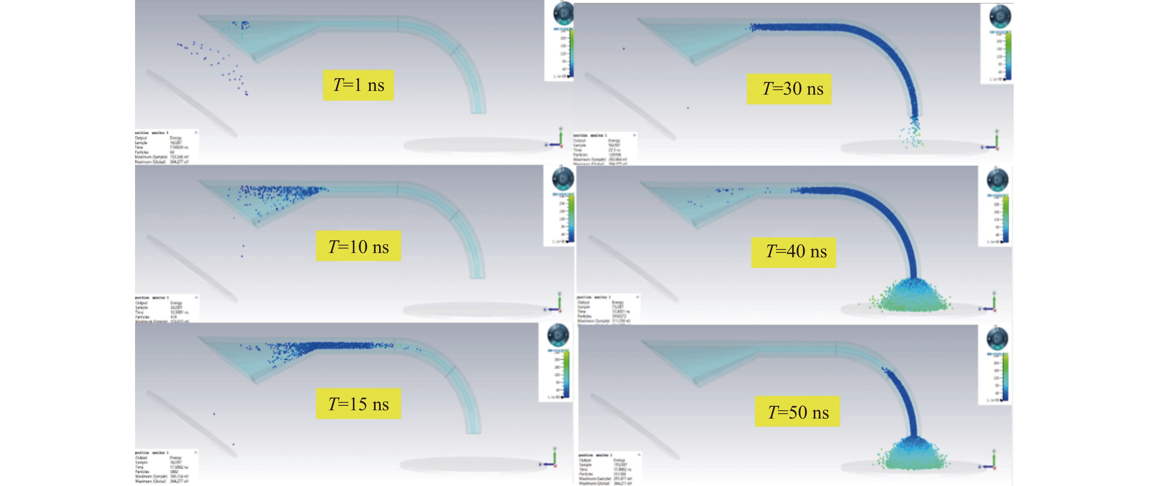
图 5 CEM初始模型的输出脉冲时间分布
Figure 5. Simulated Output Pulse Time Distribution of the Initial CEM Model
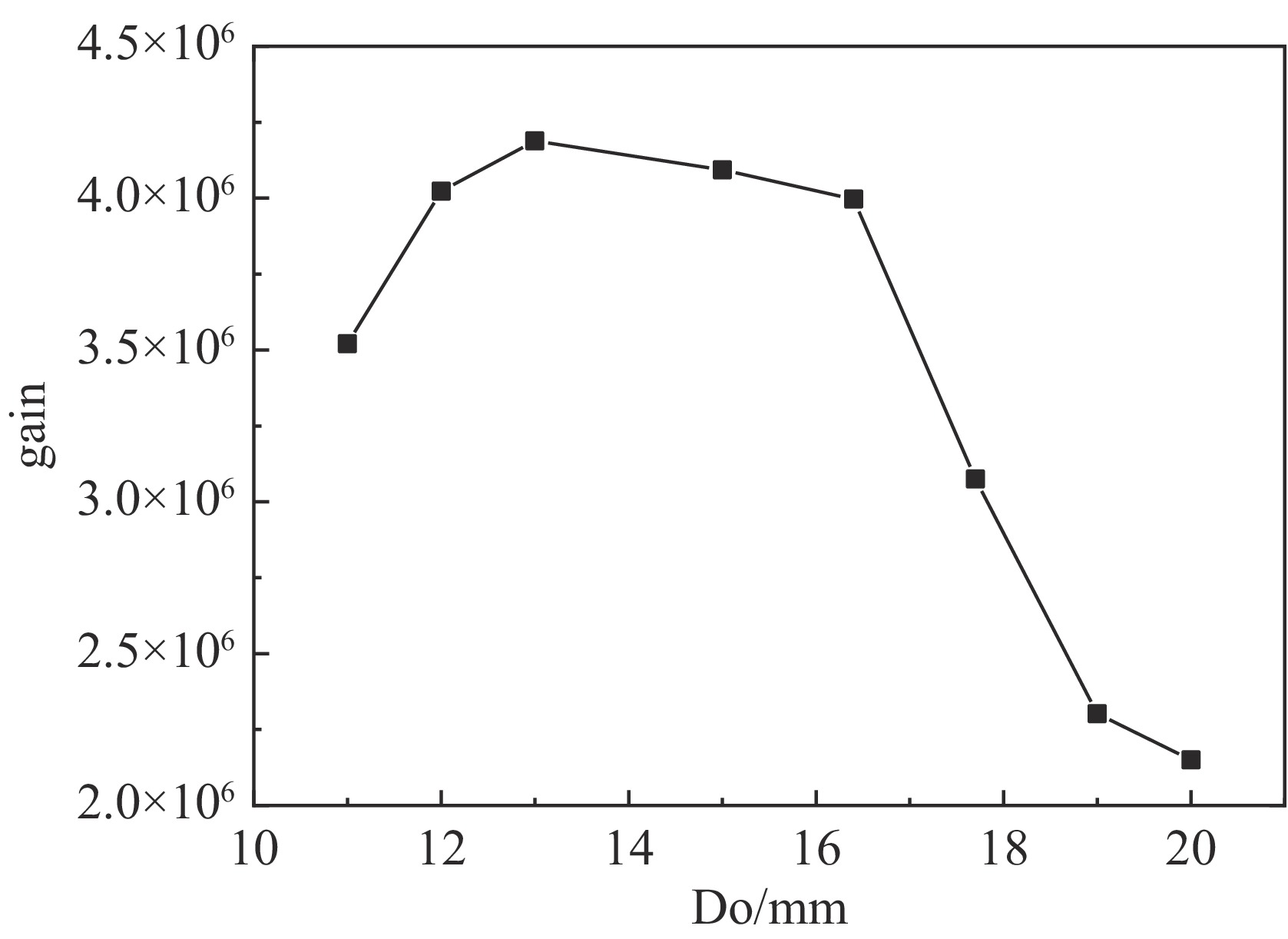
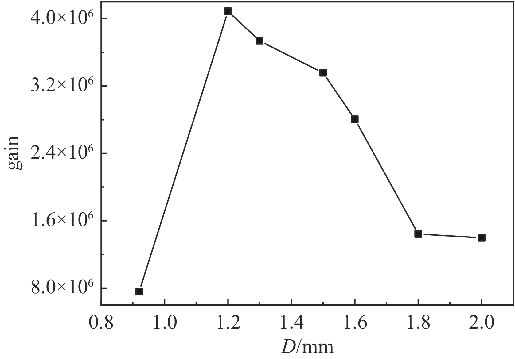
图 8 CEM喇叭口顶部宽度与增益的关系
Figure 8. Relationship Between the Top Diameter of the Bell-Shaped Aperture and the CEM Gain
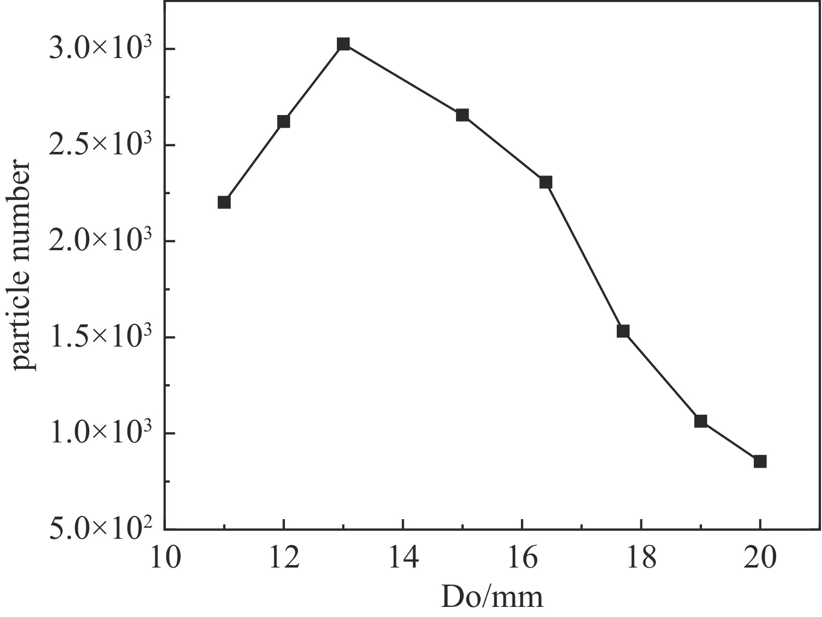
图 9 进入CEM通道电子个数与喇叭口顶部宽度的关系
Figure 9. Relationship between the number of electrons entering the CEM channel and the horn diameter
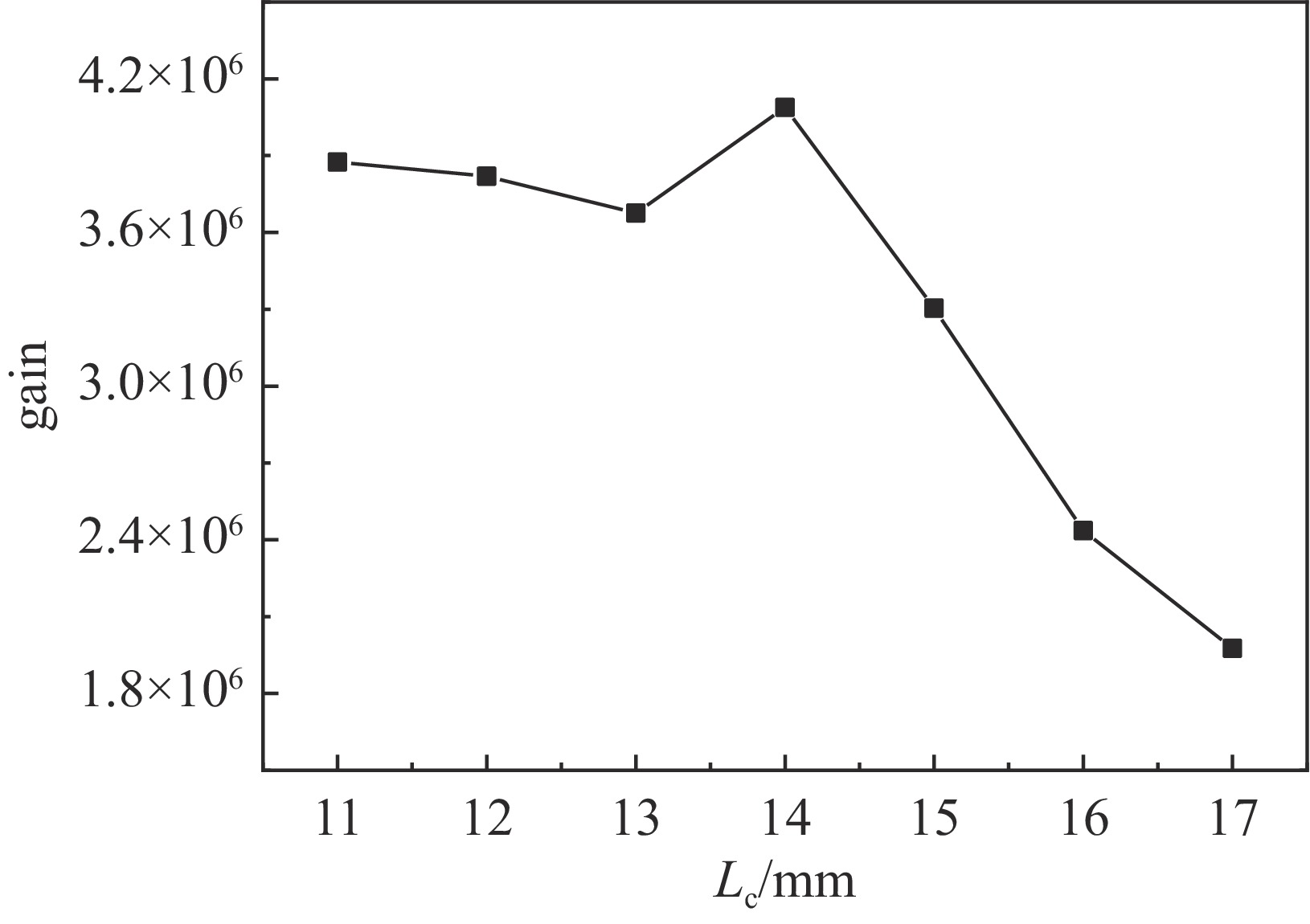
图 10 增益与平直段通道长度Lc的关系
Figure 10. Correlation of Gain with the Length of the Straight Channel Section (Lc)
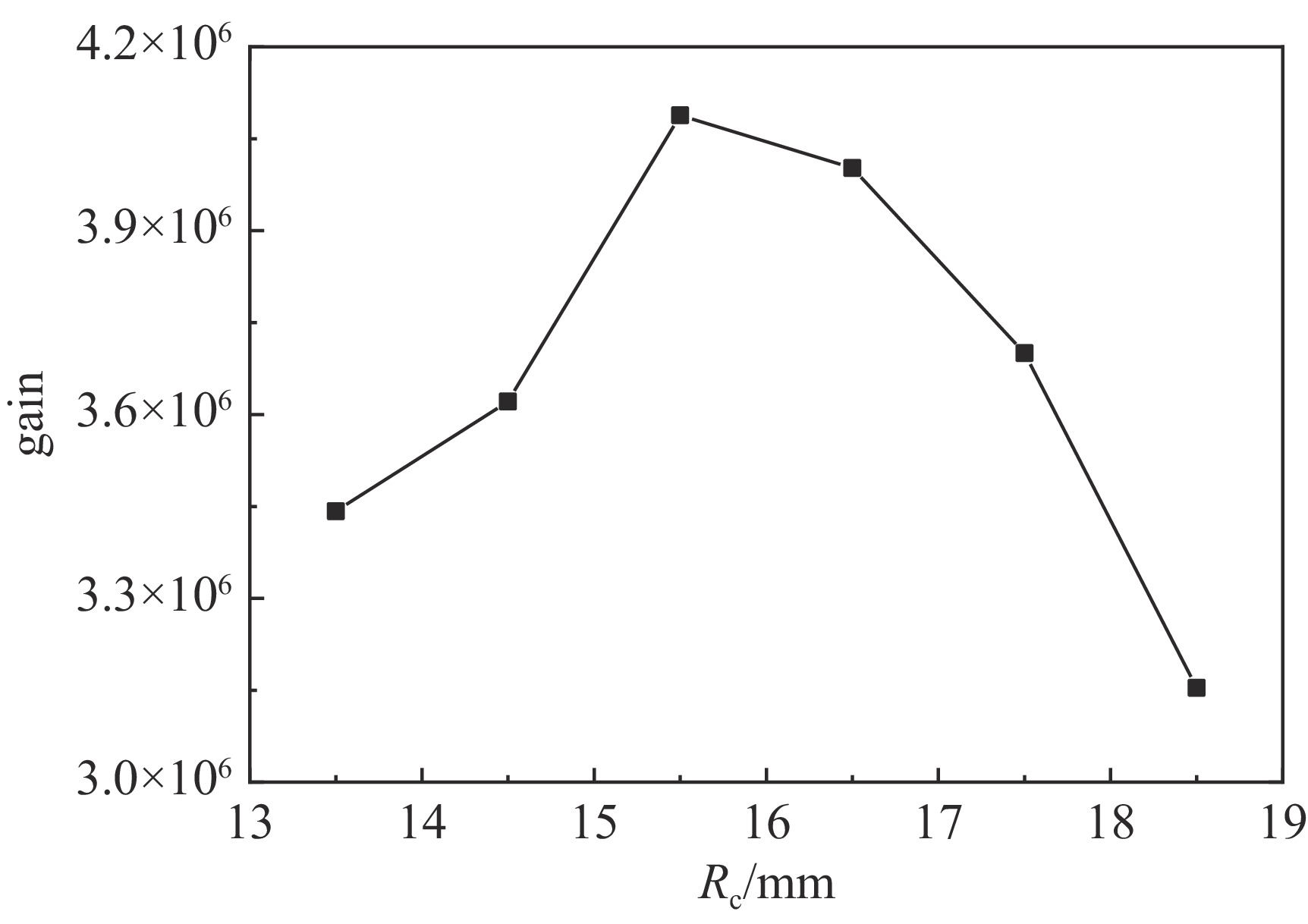
图 11 增益与弯曲通道半径Rc的关系
Figure 11. Correlation of Gain with the Radius of the Curved Channel (Rc)
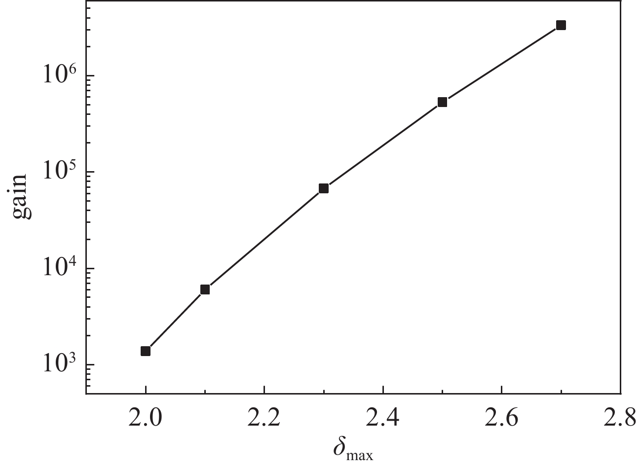
图 12 CEM二次电子发射系数δ与增益的关系
Figure 12. Dependence of the Gain on the Secondary Electron Emission Coefficient (δ) of CEM
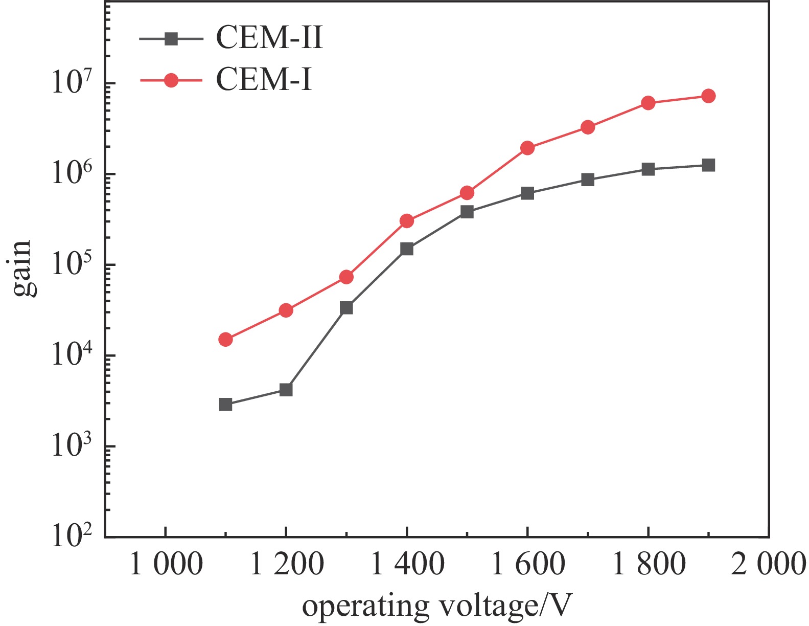
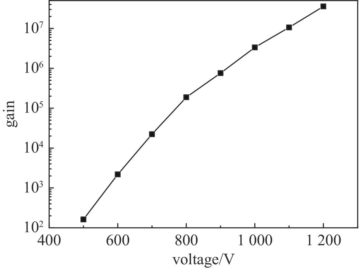
图 17 不同结构参数CEM直流测试条件下增益曲线
Figure 17. Gain Curves under CEM DC Testing Conditions for Different Structural Parameters
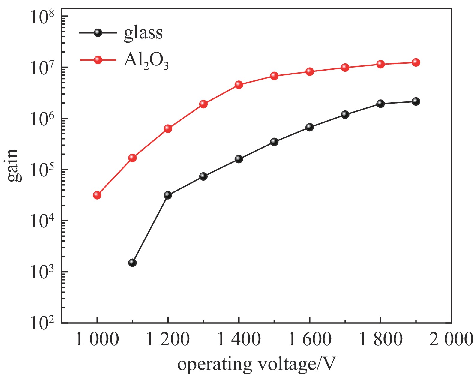
图 18 Al2O3沉积前后CEM直流测试条件下增益曲线
Figure 18. Gain Curves under CEM DC Testing Conditions Before and After Al2O3 Deposition
表 1 CEM的输入参数
Table 1. Input Parameters for the CEM
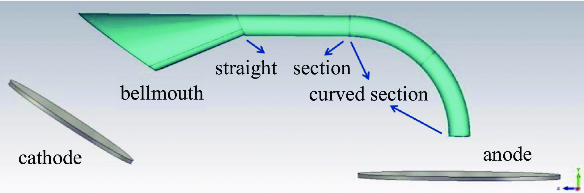
input parameters input value cathode voltage (Uc) 0 V input voltage of CEM (UCEM-in) 100 V output voltage of CEM (UCEM-out) 1000 Vanode voltage (Ua) 1100 Vvolume resistance (R) 60 MΩ channel aperture (D) 0.92 mm length of CEM (L) 52.7 mm height of CEM (L) 15.5 mm the width of the top of the bellmouth (Do) 13 mm the length of the bellmouth (Lo) 20 mm length of the straight section of CEM (Lc) 14 mm radius of the curved section of CEM (Rc) 15.5 mm  下载: 导出CSV
-
[1] Adams J, Manley B W. The mechanism of channel electron multiplication[J]. IEEE Transactions on Nuclear Science, 1966, 13(3): 88-99. doi: 10.1109/TNS.1966.4324084 [2] 张多明. 通道电子倍增器[J]. 物理, 1986(10): 635-637Zhang Duoming. Channel electron multipliers[J]. Physics, 1986(10): 635-637 [3] MacDonald E A, Thomsen M F, Funsten H O. Background in channel electron multiplier detectors due to penetrating radiation in space[J]. IEEE Transactions on Nuclear Science, 2006, 53(3): 1593-1598. doi: 10.1109/TNS.2006.874497 [4] Krems M, Zirbel J, Thomason M, et al. Channel electron multiplier and channelplate efficiencies for detecting positive ions[J]. Review of Scientific Instruments, 2005, 76: 093305. doi: 10.1063/1.2052052 [5] André N, Fedorov A, Chassela O, et al. Detection efficiency of micro channel plates and channel electron multiplier detectors to penetrating radiation in space[C]//Proceedings of the SPIE 11180, International Conference on Space Optics-ICSO 2018. 2018: 111806O. [6] Funsten H O, Harper R W, Dors E E, et al. Comparative response of microchannel plate and channel electron multiplier detectors to penetrating radiation in space[J]. IEEE Transactions on Nuclear Science, 2015, 62(5): 2283-2293. doi: 10.1109/TNS.2015.2464174 [7] Newson D M, Shipman M, Brawley S J, et al. Detection of low-energy charged particles by channel electron multipliers[J]. Journal of Instrumentation, 2022, 17: P11026. doi: 10.1088/1748-0221/17/11/P11026 [8] Tassotto M, Watson P R. Detection efficiency of a channel electron multiplier for low energy incident noble gas ions[J]. Review of Scientific Instruments, 2000, 71(7): 2704-2709. doi: 10.1063/1.1150678 [9] 张斌婷, 刘术林, 闫保军, 等. 单螺旋通道的通道电子倍增器性能研究[J]. 核技术, 2023, 46: 100403 doi: 10.11889/j.0253-3219.2023.hjs.46.100403Zhang Binting, Liu Shulin, Yan Baojun, et al. Performance of channel electron multiplier with single helix channel[J]. Nuclear Techniques, 2023, 46: 100403 doi: 10.11889/j.0253-3219.2023.hjs.46.100403 [10] Chen Lin, Wang Xingchao, Qian Sen, et al. Optimizing the design of ultrafast photomultiplier tubes[J]. Optics Express, 2023, 31(18): 29975-29985. doi: 10.1364/OE.498230 [11] Chen Lin, Luo Ting, Wang Xingchao, et al. Simulation design of a new MCP-PMT with large photocathode area and high time resolution[J]. IEEE Transactions on Nuclear Science, 2024, 71(4): 884-887. doi: 10.1109/TNS.2024.3376350 [12] Qian Sen, Wu Qi, Ma Lishuang, et al. Simulation of FPMT with single chip MCP[J]. Journal of Physics: Conference Series, 2022, 2374: 012135. doi: 10.1088/1742-6596/2374/1/012135 [13] Li Lili, Tian Jinshou, Chen Ping, et al. Numerical simulation on magnetic field tolerance of MCP-PMTs[J]. IEEE Transactions on Nuclear Science, 2022, 69(4): 850-857. doi: 10.1109/TNS.2022.3150890 -

 点击查看大图
计量
- 文章访问数: 33
- HTML全文浏览量: 11
- PDF下载量: 4
- 被引次数: 0
