

Simulation of SiC based turn-off light initiated multi gate semiconductor switches
-
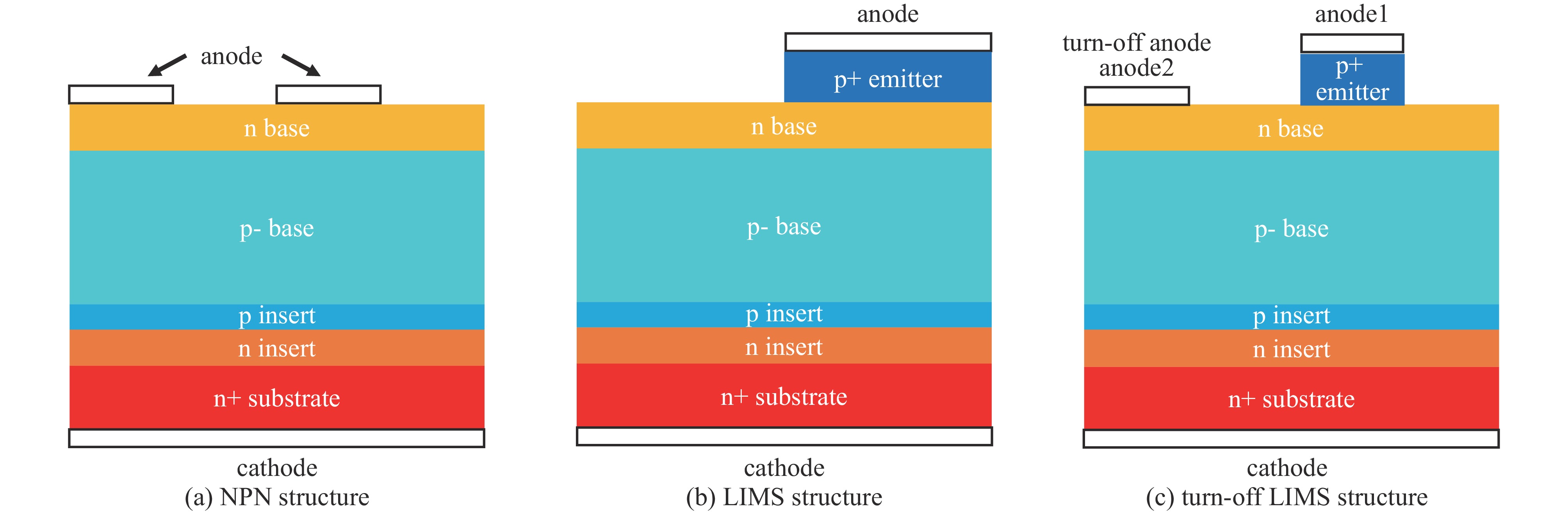
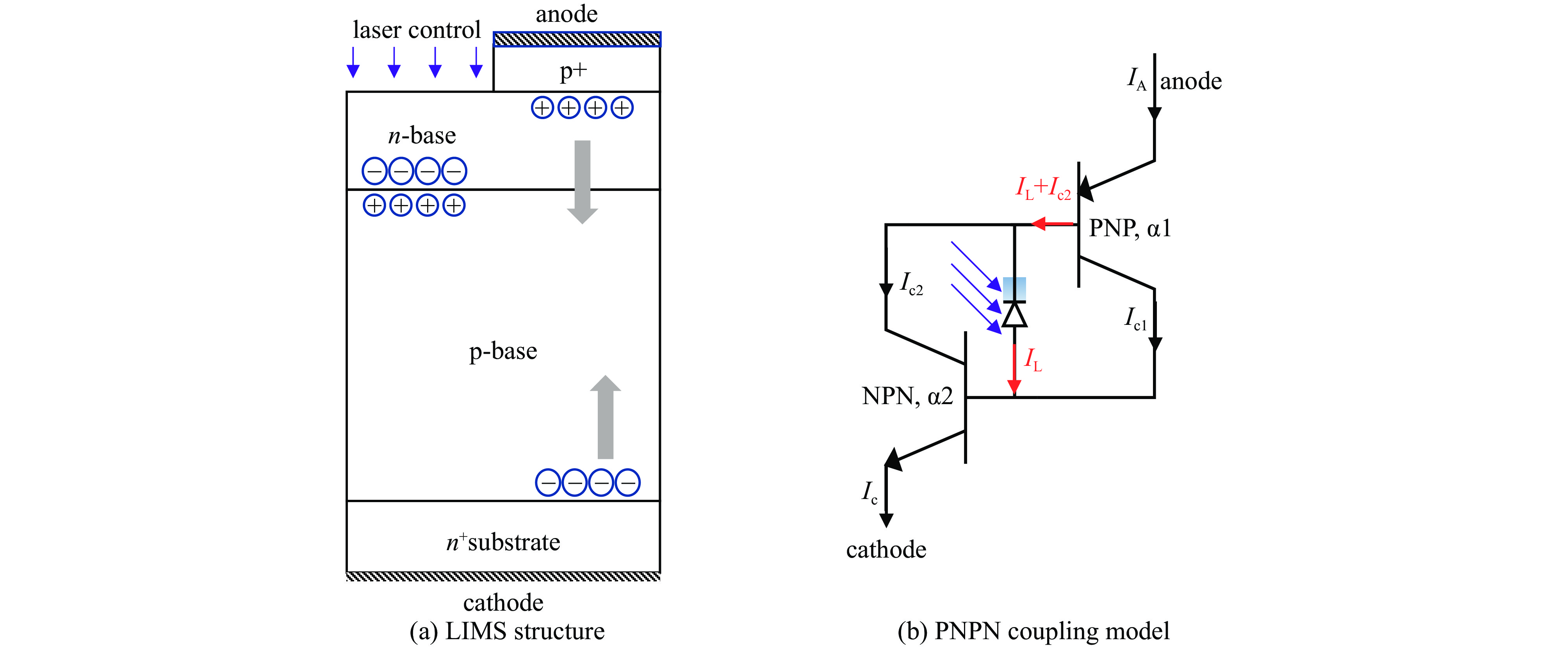
摘要: 碳化硅(SiC)基光触发多门极半导体开关(LIMS)具有功率容量高,导通速度快的显著优势,在雷达、加速器以及脉冲源等方面广泛应用。针对LIMS存在的下降沿长,关断速度慢等问题,提出了一种具有关断作用的LIMS阳极结构设计。通过实验数据对仿真模型进行校准,并结合仿真对具有关断阳极结构器件的导通特性进行研究。仿真结果表明,具有关断阳极结构的器件,能在激光触发后形成pnpn结构的正反馈效应,增加导通电流。在激光结束后,随着光生载流子的复合,以及关断阳极结构对基区载流子的抽取作用,显著地提高器件的关断速度。当输入电压为4 kV时,在数百A脉冲电流放电条件下,电流脉冲宽度从0.79 μs减小到百ns以下,器件的关断时间降低至0.6 μs,可以在kHz及以上的重复频率场景中应用。
-
关键词:
- 碳化硅 /
- 光触发多门极半导体开关 /
- 阳极结构 /
- 关断速度
Abstract:Background SiC-based light-initiated multi-gate semiconductor switches (LIMS) deliver superior response speeds due to the faster injection of photo-generated carriers compared to conventional electrically injected carriers. They can be used in a variety of applications, including radars, accelerators, and pulse sources.Purpose Regarding the problems such as the long falling edge and slow turn-off speed of LIMS, an anode structure design with turn-off capability is proposed.Methods The model and its parameters are calibrated based on experimental data, and the simulation is used to study the conduction characteristics of devices with a turn-off anode structure.Results The simulation results show that devices with a turn-off anode structure can achieve positive feedback in the pnpn configuration following laser activation, thereby increasing the conduction current. When the laser pulse ends, the recombination of photo-generated carriers and the extraction of carriers from the base region by the turn-off anode structure significantly enhance the turn-off speed of the device.Conclusions With a 4 kV anode bias and a peak current of several hundred amperes, the modified LIMS reduces the full-width-at-half-maximum of the current pulse from 0.79 µs to <100 ns and shortens the turn-off time to 0.6 µs. These results indicate suitability for repetitive operation at kilohertz frequencies and above. -
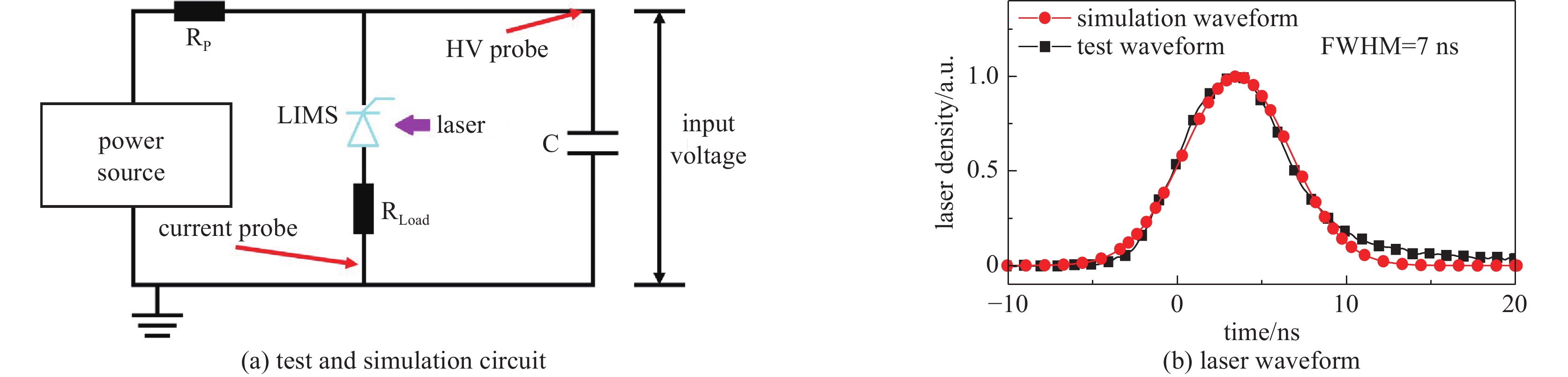
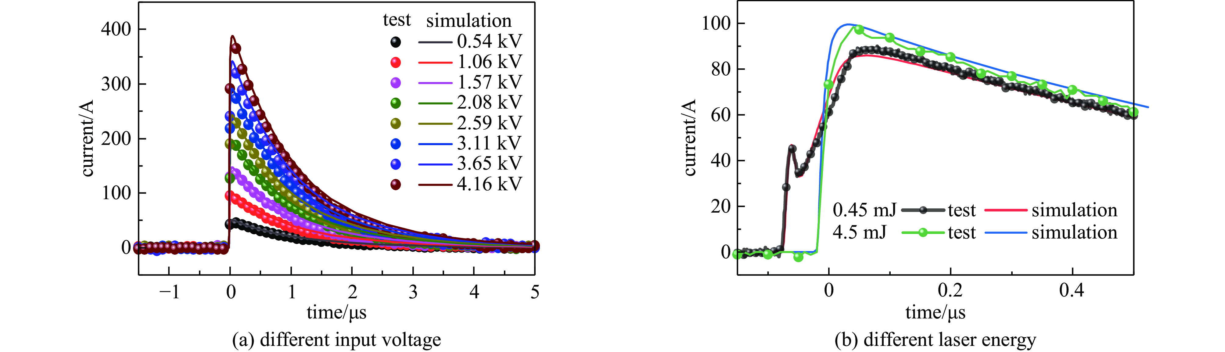
图 2 LIMS导通性能电路以及激光波形示意图
Figure 2. The circuits and laser waveform for the on-state of the LIMS
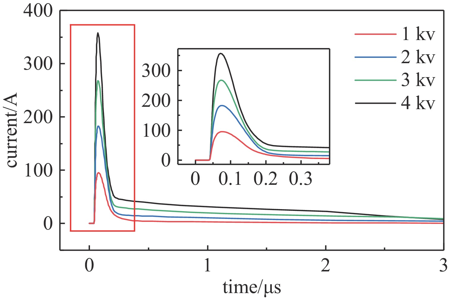
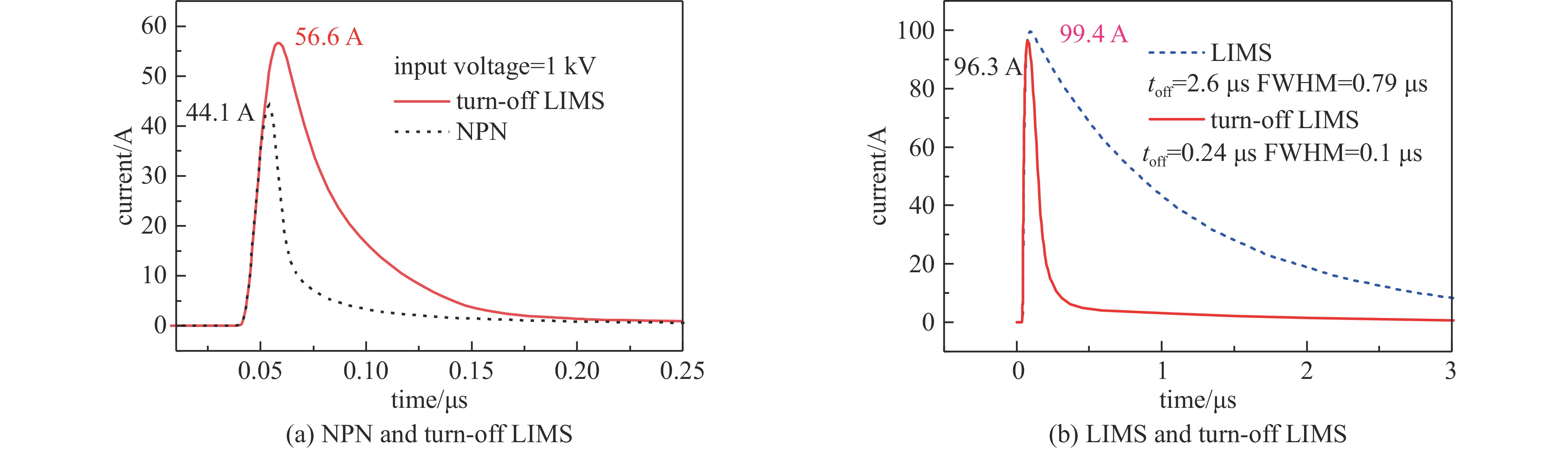
图 6 不同电压下可关断LIMS器件的瞬态响应曲线
Figure 6. Transient responses of turn-off LIMS under different voltages
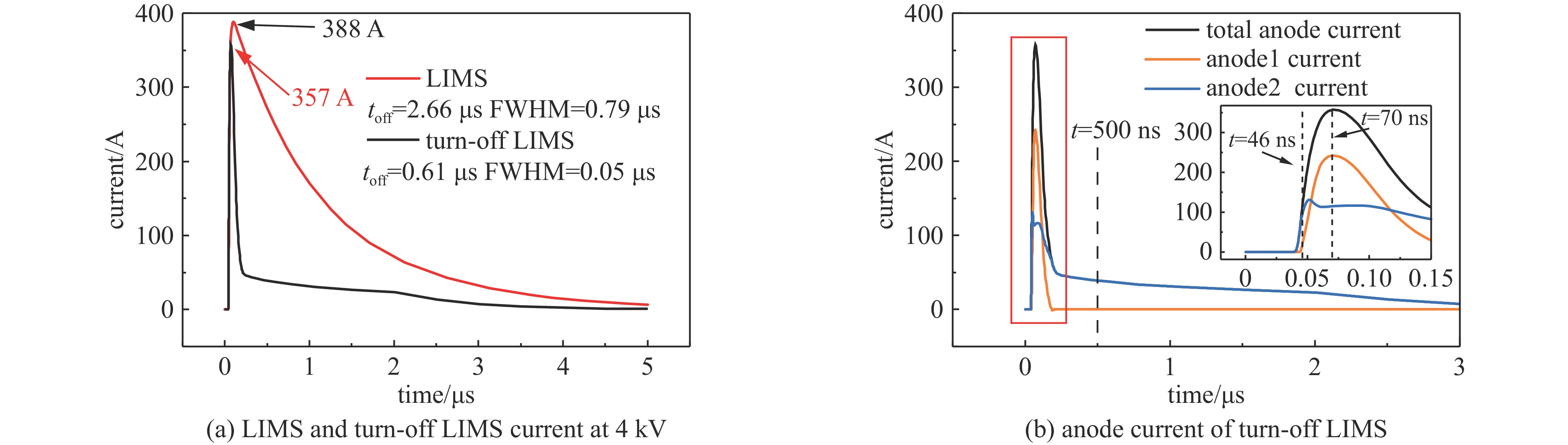
图 7 输入电压为4 kV时,LIMS和可关断LIMS器件的瞬态响应曲线
Figure 7. The transient responses of LIMS and turn-off LIMS at input voltage of 4 kV
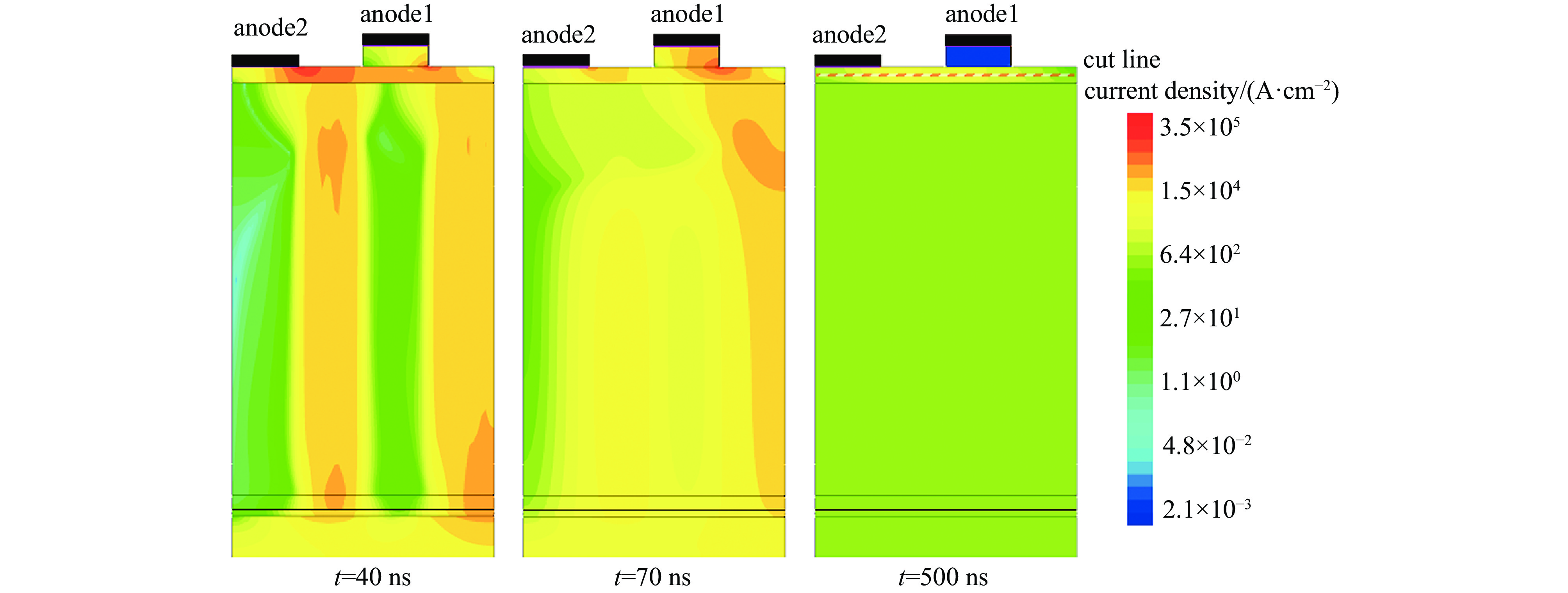
图 8 可关断LIMS器件导通时的电流密度分布
Figure 8. Current density distribution at on-state of turn-off LIMS
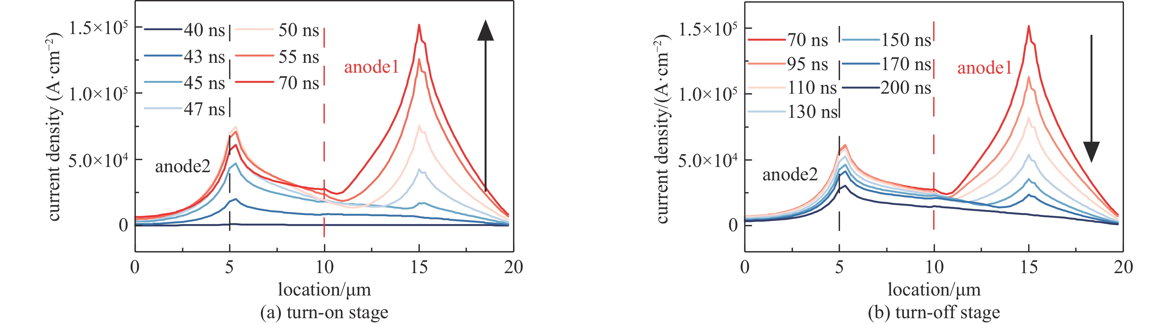
图 9 可关断LIMS器件开启和关断阶段电流密度分布
Figure 9. Current density distribution during the turn-on and turn-off stages of the device
表 1 碳化硅LIMS仿真参数
Table 1. Parameters for simulation of SiC LIMS
semiconductor
band gap/eVdielectric
constantμn/(cm2·V−1·s−1) μp/(cm2·V−1·s−1) absorption
coefficient/cm−1τn/μs τp/μs saturation drift
velocity/(cm·s−1)3.4 9.76 950 125 200 1 0.2 2×10  下载: 导出CSV
表 2 碳化硅掺杂浓度和厚度
Table 2. Doping and thickness of SiC
layer doping concentration/cm−3 thickness/μm p+ emitter 1.5×10¹⁹ 3 n base 3.0×10¹⁷ 2.5 p- base 4.0×10¹⁴ 60 p insert 5.0×10¹⁶ 2 n insert 3.0×10¹⁸ 1 n+ substrate 5.0×10¹⁹ 350
下载: 导出CSV
-
[1] 梁琳, 颜小雪, 黄鑫远, 等. 半导体脉冲功率开关器件综述[J]. 中国电机工程学报, 2022, 42(23): 8631-8651Liang Lin, Yan Xiaoxue, Huang Xinyuan, et al. Review on semiconductor pulsed power switching devices[J]. Proceedings of the CSEE, 2022, 42(23): 8631-8651 [2] 邵方格. SiC GTO器件的驱动设计与优化[D]. 杭州: 浙江大学, 2023: 6-9Shao Fangge. Driver design and optimization of SiC GTO devices[D]. Hangzhou: Zhejiang University, 2023: 6-9 [3] 孙瑞泽, 陈万军, 刘超, 等. 压控型脉冲功率半导体器件技术及应用[J]. 强激光与粒子束, 2024, 36: 095001 doi: 10.11884/HPLPB202436.240120Sun Ruize, Chen Wanjun, Liu Chao, et al. Technology and application of the voltage-controlled pulse power semiconductor devices[J]. High Power Laser and Particle Beams, 2024, 36: 095001 doi: 10.11884/HPLPB202436.240120 [4] Kimoto T, Cooper J A. Fundamentals of silicon carbide technology: growth, characterization, devices, and applications[M]. Singapore: John Wiley & Sons Singapore Pte. Ltd, 2014. [5] Rafin S M S H, Ahmed R, Haque M A, et al. Power electronics revolutionized: a comprehensive analysis of emerging wide and ultrawide bandgap devices[J]. Micromachines, 2023, 14: 2045. doi: 10.3390/mi14112045 [6] 龙虎. 10kV碳化硅二极管与晶闸管的终端技术研究[D]. 杭州: 浙江大学, 2023: 10-31Long Hu. Study on termination technologies of 10-kV silicon carbide diodes and thyristors[D]. Hangzhou: Zhejiang University, 2023: 10-31 [7] 周才能, 岳瑞峰, 王燕. 碳化硅门极可关断晶闸管的研究进展[J]. 半导体技术, 2016, 41(2): 89-95Zhou Caineng, Yue Ruifeng, Wang Yan. Research Developments in silicon carbide gate turn-off thyristors[J]. Semiconductor Technology, 2016, 41(2): 89-95 [8] 张渊. 6500V碳化硅发射极关断晶闸管仿真和特性的研究[D]. 长沙: 湖南大学, 2017: 10-12Zhang Yuan. Research on 6500V SiC ETO simulation and characteristics[D]. Changsha: Hunan University, 2017: 10-12 [9] 陈楠. 3300V MOS控制晶闸管设计与实现[D]. 成都: 电子科技大学, 2021: 15-22Chen Nan. Design and realization of a 3300V MOS controlled thyristor[D]. Chengdu: University of Electronic Science and Technology of China, 2021: 15-22 [10] 钟艺文. SiC MOS控制晶闸管的机理研究与特性分析[D]. 西安: 西安理工大学, 2022: 9-12Zhong Yiwen. Mechanism research and characteristic analysis of SiC MOS controlled thyristor[D]. Xi’an: Xi’an University of Technology, 2022: 9-12 [11] 刘中梦雪, 黄伟, 刘垚, 等. 低导通压降MOS控制晶闸管的研制[J]. 半导体技术, 2023, 48(6): 476-481,487 doi: 10.13290/j.cnki.bdtjs.2023.06.004Liu Zhongmengxue, Huang Wei, Liu Yao, et al. Development of the MOS controlled thyristor with low on-state voltage drop[J]. Semiconductor Technology, 2023, 48(6): 476-481,487 doi: 10.13290/j.cnki.bdtjs.2023.06.004 [12] 张荣. 静电感应晶闸管的研制[D]. 兰州: 兰州大学, 2009: 4-10Zhang Rong. The research and manufacture of static induction thyristor[D]. Lanzhou: Lanzhou University, 2009: 4-10 [13] 王曦. 4H-SiC光触发晶闸管新结构研究[D]. 西安: 西安理工大学, 2019: 11-13Wang Xi. Study on novel structure of 4H-SiC light triggered thyristor[D]. Xi’an: Xi’an University of Technology, 2019: 11-13 [14] Luan Chongbiao, Yuan Jianqiang, Liu Hongwei, et al. Study of a novel SiC-based light initiated multi-gate semiconductor switch[J]. Journal of Semiconductors, 2025, 46: 112402. doi: 10.1088/1674-4926/25020033 [15] 安丽琪. SiC光触发晶闸管放大门极结构的设计与研究[D]. 西安: 西安理工大学, 2020: 7-11An Liqi. Design and study of SiC light triggered thyristor amplified gate structure[D]. Xi’an: Xi’an University of Technology, 2020: 7-11 [16] 刘宏伟, 王凌云, 栾崇彪, 等. 激光触发多门极半导体开关初步研究[J]. 强激光与粒子束, 2024, 36: 115004 doi: 10.11884/HPLPB202436.240331Liu Hongwei, Wang Lingyun, Luan Chongbiao, et al. Preliminary study on laser initiated multi-gate semiconductor switch[J]. High Power Laser and Particle Beams, 2024, 36: 115004 doi: 10.11884/HPLPB202436.240331 [17] 王凌云, 刘宏伟, 袁建强, 等. 光控多门极晶闸管的多种工作模式[J]. 物理学报, 2025, 74: 058401 doi: 10.7498/aps.74.20241608Wang Lingyun, Liu Hongwei, Yuan Jianqiang, et al. Various operating modes of optically controlled multi-gate thyristors[J]. Acta Physica Sinica, 2025, 74: 058401 doi: 10.7498/aps.74.20241608 [18] 李昊. 4H-SiC JBS与GTO中子辐照损伤及其退化机理研究[D]. 兰州: 兰州大学, 2024: 20-21Li Hao. Research on neutron irradiation damage and degradation mechanism of 4H-SiC JBS and GTO[D]. Lanzhou: Lanzhou University, 2024: 20-21 [19] Ruff M, Mitlehner H, Helbig R. SiC devices: physics and numerical simulation[J]. IEEE Transactions on Electron Devices, 1994, 41(6): 1040-1054. doi: 10.1109/16.293319 [20] Hillkirk L M, Hefner A R, Dutton R W. Physics-based numerical simulation for design of high-voltage, extremely-high current density SiC power devices[C]//Proceedings of the International Semiconductor Device Research Symposium. 2007: 1-2. [21] Galeckas A, Linnros J, Grivickas V, et al. Auger recombination in 4H-SiC: Unusual temperature behavior[J]. Applied Physics Letters, 1997, 71(22): 3269-3271. doi: 10.1063/1.120309 [22] Kimoto T, Niwa H, Okuda T, et al. Carrier lifetime and breakdown phenomena in SiC power device material[J]. Journal of Physics D: Applied Physics, 2018, 51: 363001. doi: 10.1088/1361-6463/aad26a [23] Chen Shengtao, Xu Ming, Lv Ruidong, et al. Photon absorption effects on the transient carrier dynamics in high-purity 4H-SiC PCSS[J]. IEEE Electron Device Letters, 2025, 46(2): 278-281. doi: 10.1109/LED.2024.3506561 [24] Khan I A, Cooper J A. Measurement of high-field electron transport in silicon carbide[J]. IEEE Transactions on Electron Devices, 2000, 47(2): 269-273. doi: 10.1109/16.822266 -

 点击查看大图
计量
- 文章访问数: 24
- HTML全文浏览量: 8
- PDF下载量: 3
- 被引次数: 0
