

Electrothermal characterization model for the micro-contact interface of pulse thyristors
-
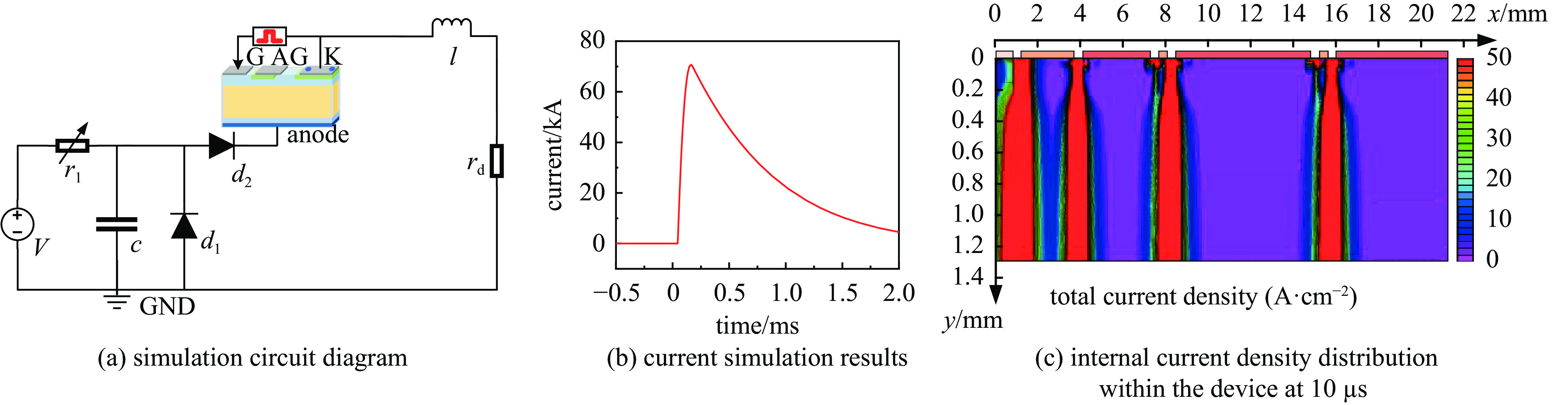
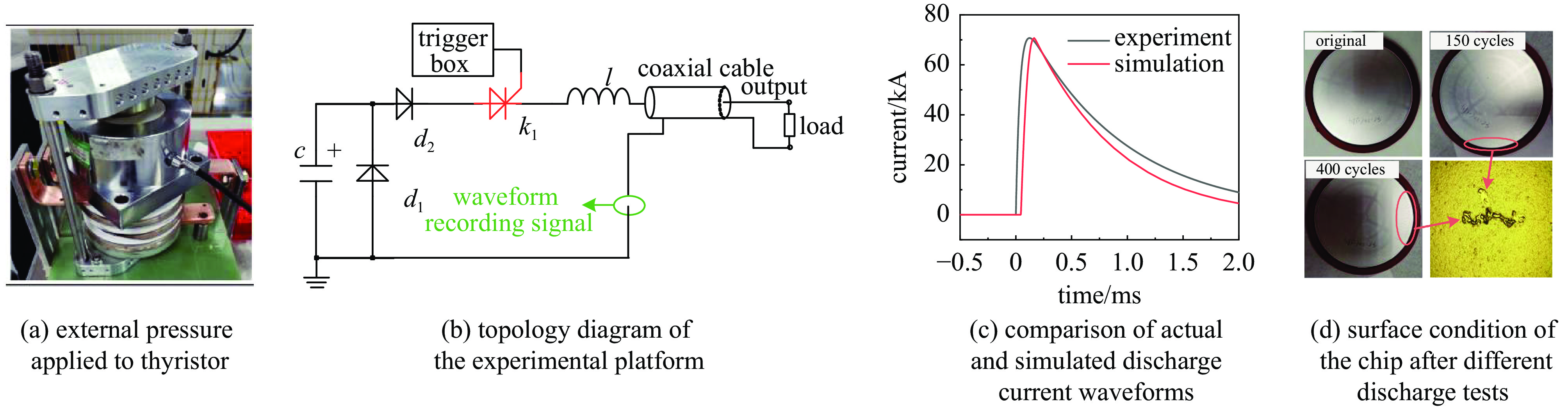
摘要: 脉冲晶闸管工作在强流脉冲工况,重复的电磁热力联合冲击会导致局部过温造成铝层电熔蚀、进而加速晶闸管热疲劳失效。针对由于接触界面电热效应产生的失效问题,综合考虑表面粗糙度、外施压力、电极图案和载流子扩散等因素,建立了脉冲晶闸管微观接触界面电热特性表征模型,并在脉冲工况下进行了仿真模拟。设计了晶闸管电熔蚀加速老化试验验证仿真的正确性,在重复放电140次时,开关阳极表面外圈出现明显铝层熔蚀现象;当放电次数达到400次时,硅坑在更靠近门极位置出现。试验结果证明了模型对电熔蚀失效规律的预测精度,为脉冲晶闸管电熔蚀失效的定量评估提供了可靠技术支撑。Abstract:
Background Pulse thyristors operate under high-current pulse conditions, where repeated combined electromagnetic and thermal stresses cause localised overheating. This leads to electrothermal erosion of the aluminum layer, accelerating thermal fatigue failure of the thyristor.Purpose This study aims to establish an electrothermal characterization model to evaluate the electro-erosion effect, thereby providing reliable technical support for the quantitative assessment of pulse thyristor electrical erosion failures.Methods A micro-scale contact interface electrothermal characteristic characterization model for pulse thyristors was established. This model comprehensively considers factors such as surface roughness, applied pressure, electrode patterns, and carrier diffusion, and was simulated under pulsed operating conditions. Furthermore, an accelerated aging test for thyristor electro-erosion was designed to validate the simulation's accuracy.Results Experimental observations revealed that after 140 repeated discharges, significant aluminum layer erosion appeared on the outer ring of the switch anode surface. When the discharge cycles reached 400, silicon pits emerged closer to the gate position.Conclusions The experimental results successfully validated the model's predictive accuracy regarding the failure mechanisms of electrical erosion. This proposed model provides reliable technical support for the quantitative assessment of pulse thyristor electrical erosion failures. -
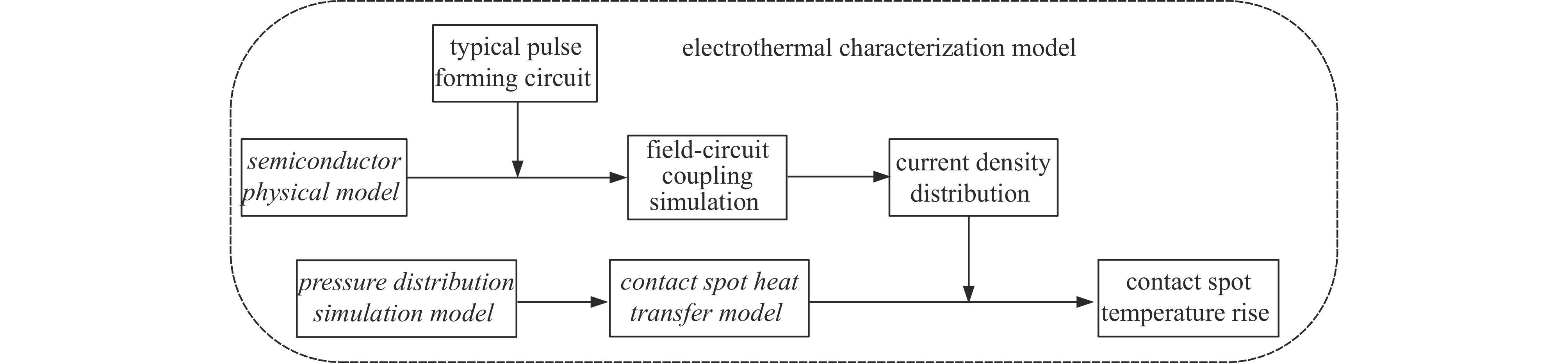
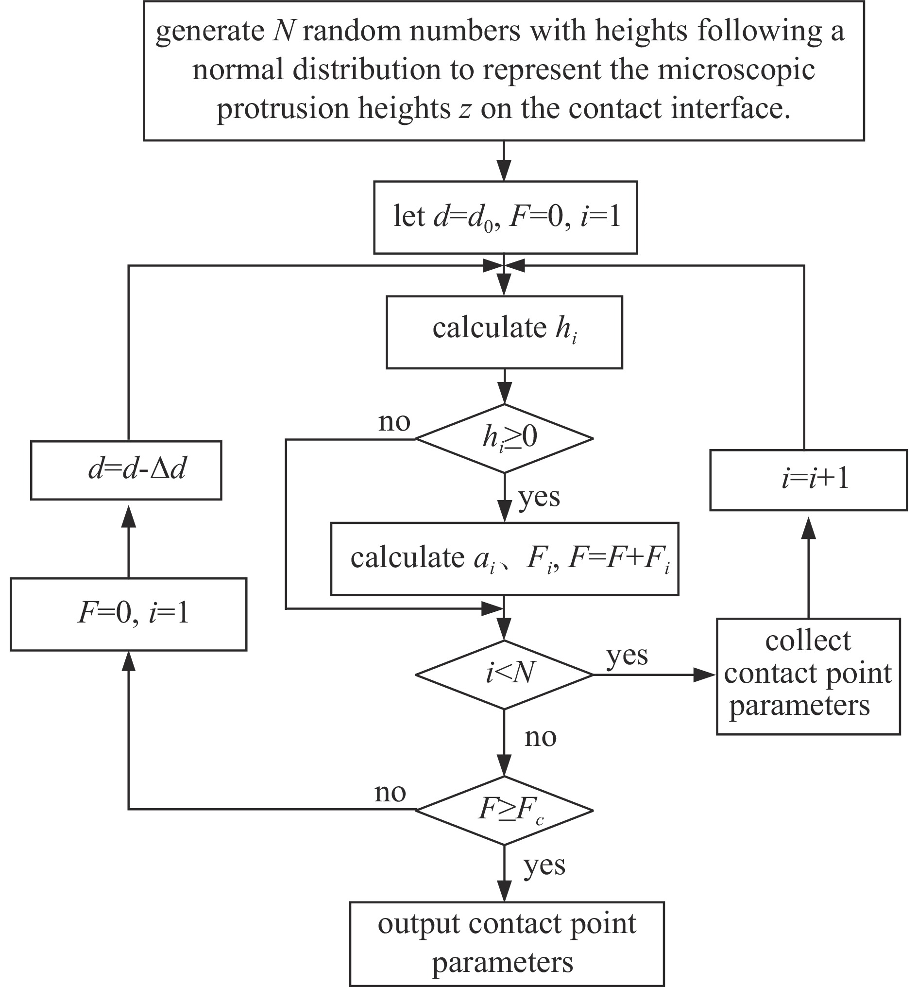
图 1 脉冲晶闸管微观接触界面电热特性表征模型建模思路
Figure 1. Approach for electrothermal characterization model for the micro-contact interface of pulse thyristors
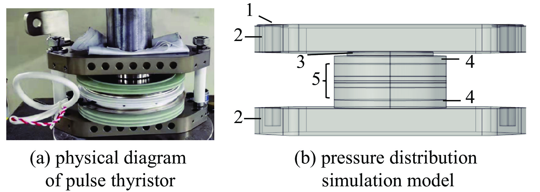
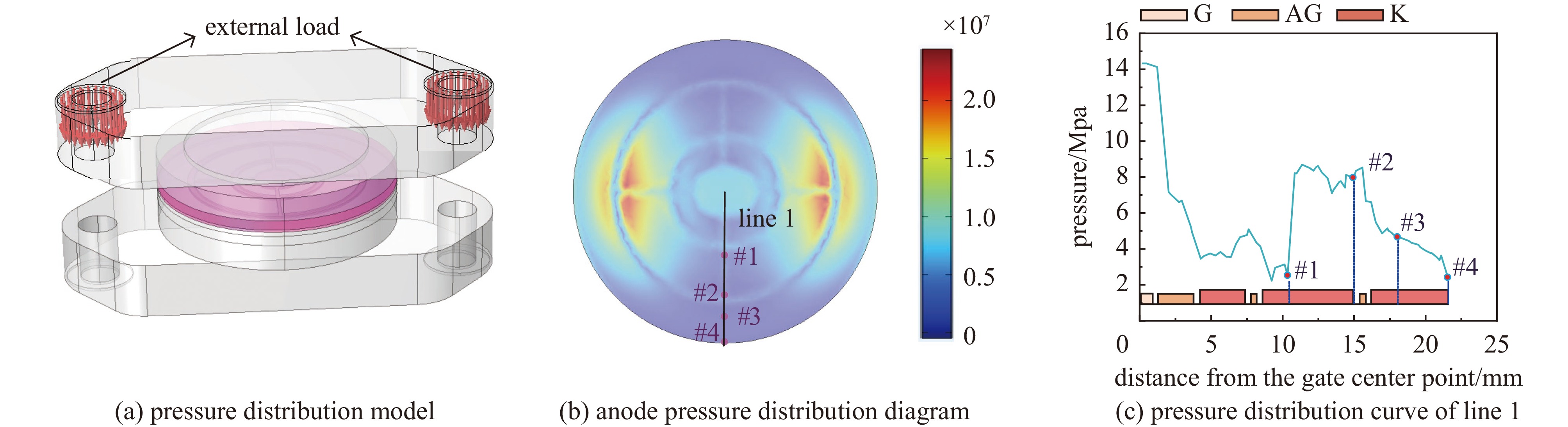
图 2 脉冲晶闸管实物及压力分布仿真模型
Figure 2. Pulse thyristor physical model and pressure distribution simulation model

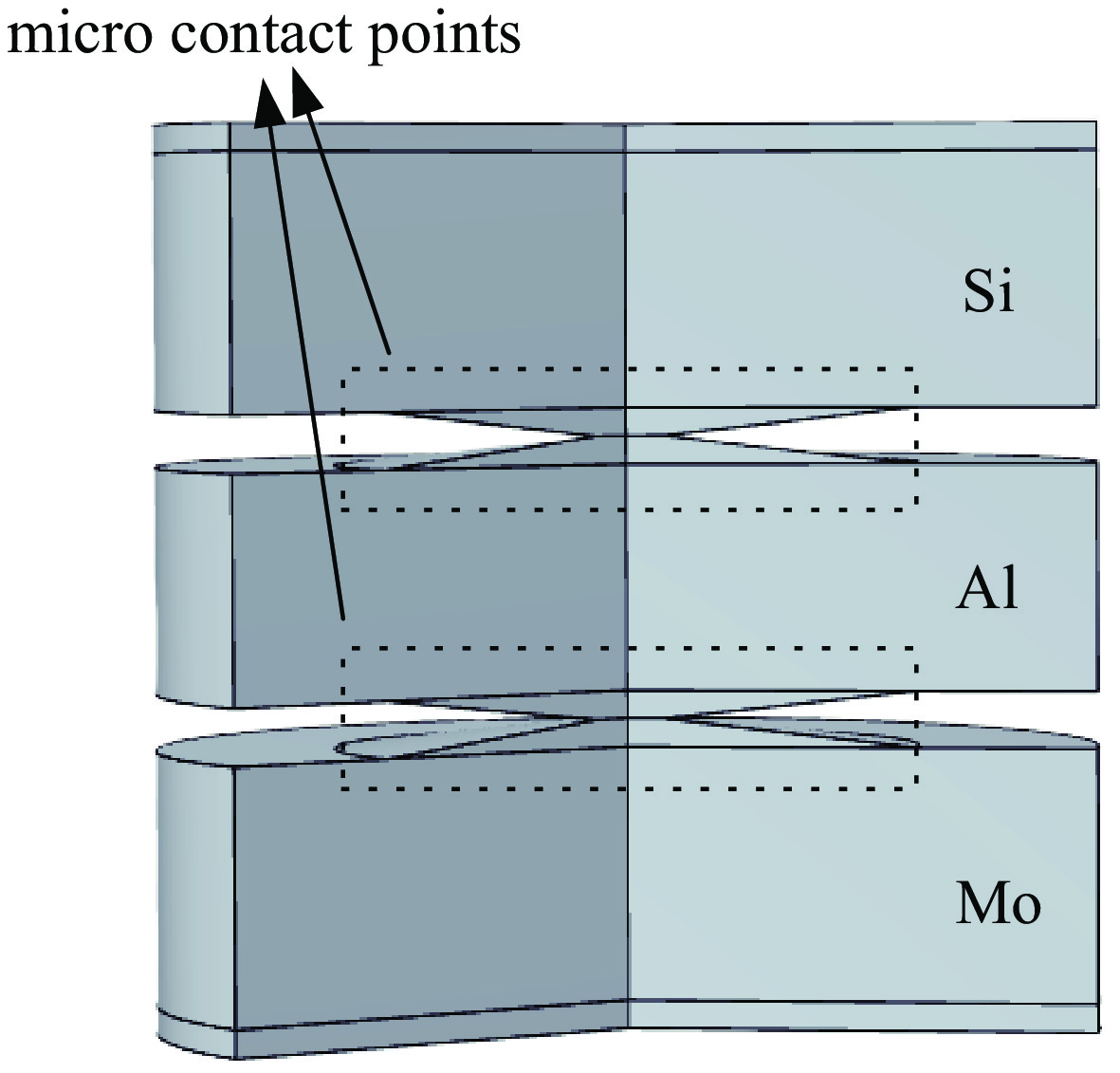
图 3 接触面及单个接触斑点示意图
Figure 3. Schematic diagram of the contact interface and a single contact spot
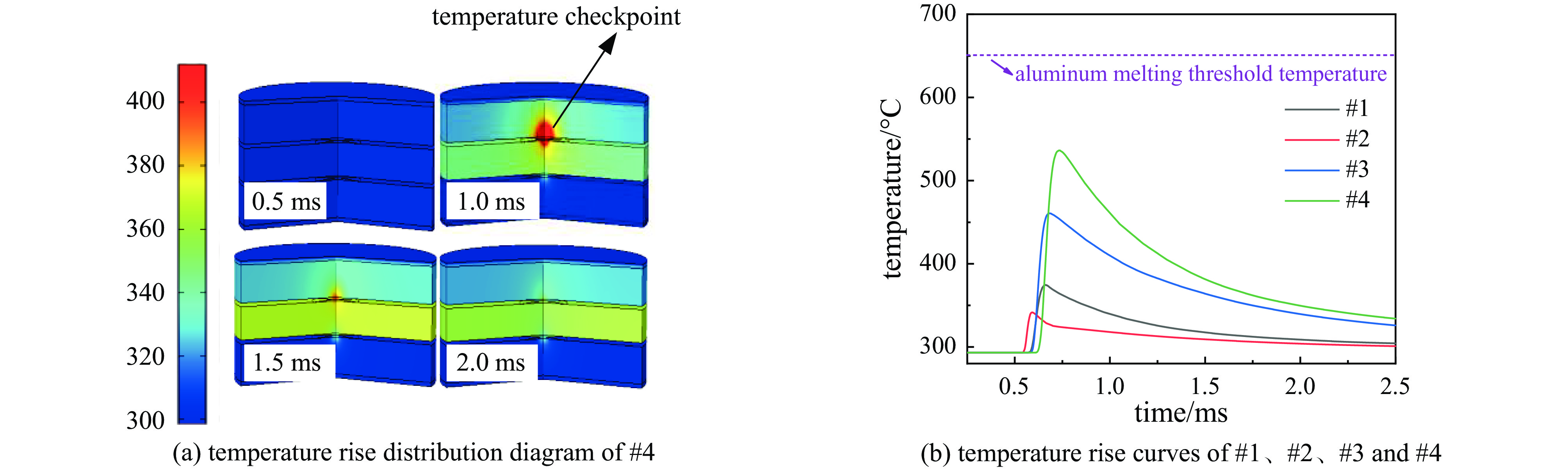
图 11 接触斑点热特性仿真结果
Figure 11. Simulation results of the thermal characteristics of contact spots
表 1 压力分布模型各组件材料
Table 1. Materials for each component of the pressure distribution model
No. name materials 1 gasket 304 stainless steel 2 clamping plate 7075 aluminum alloy3 shim 45 steel 4 simplified assembly copper 5 pulse thyristor Silicon, molybdenum, copper  下载: 导出CSV
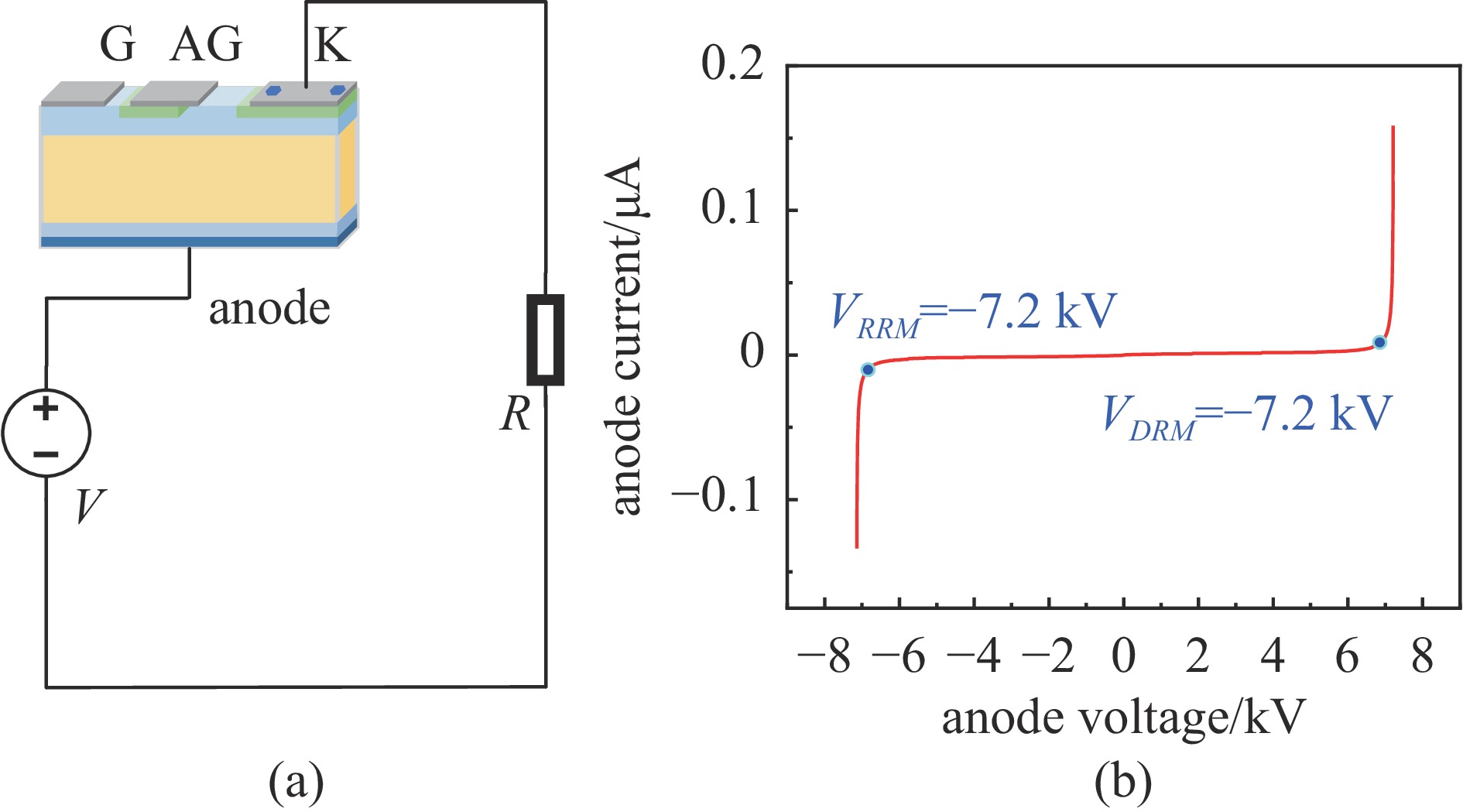
表 2 部分技术参数
Table 2. Partial technical parameters
repetitive peak off-state voltage VDRM/V critical rate of rise of off-state voltage (dv/dt)/(V·μs−1) gate trigger current IGT/mA 5600 ~6500 2000 40
下载: 导出CSV
表 3 接触面材料物理参数
Table 3. Physical parameters of the contact surface material
material Poisson’s
ratioelastic modulus/
GParesistivity/
(Ω·m)specific heat capacity/
(J·kg−3·K−3)density/(kg·m−3) melting point/℃ aluminum 0.33 71.7 2.7×10⁻⁹ 900 2690 660 silicon 0.28 190 1.9×10⁻³ 700 2329 1410 molybdenum 0.32 320 5.2×10⁻⁹ 242.8 10200 2620
下载: 导出CSV
表 4 接触斑点尺寸参数
Table 4. Contact spot size parameter
contact spot number pressure/(N·m−2) base radius of the micro-unit/μm a/μm d/μm #1 2.2×10⁶ 136.8 2.5 1.41 #2 8.3×10⁶ 87.1 3.0 1.06 #3 4.5×10⁶ 105.1 2.7 1.22 #4 2.5×10⁶ 133.2 2.6 1.38
下载: 导出CSV
-
[1] 张星汝, 冯冰洋, 刘俊, 等. 高电压大电流晶闸管组件的热特性[J]. 强激光与粒子束, 2020, 32: 025016 doi: 10.11884/HPLPB202032.190346Zhang Xingru, Feng Bingyang, Liu Jun, et al. Thermal characteristics of high voltage and high current thyristor assembly[J]. High Power Laser and Particle Beams, 2020, 32: 025016 doi: 10.11884/HPLPB202032.190346 [2] Liu Yi, Lin Fuchang, Dai Ling, et al. Development of a compact 450-kJ pulsed-power-supply system for electromagnetic launcher[J]. IEEE Transactions on Plasma Science, 2011, 39(1): 304-309. doi: 10.1109/TPS.2010.2050339 [3] Taylor P D. 晶闸管的设计与制造[M]. 庞银锁, 译. 北京: 中国铁道出版社, 1992Taylor P D. Thyristor design and realization[M]. Pang Yinsuo, trans. Beijing: China Railway Publishing House, 1992 [4] 缪云欣. 脉冲晶闸管型强流开关电熔蚀失效特性研究[D]. 武汉: 华中科技大学, 2024Miao Yunxin. Research on failure characteristics due to electrical melting erosion in heavy current switches based on pulse thyristor[D]. Wuhan: Huazhong University of Science and Technology, 2024 [5] 李辉, 余越, 姚然, 等. 基于多层级模拟的压接型IGBT器件短路失效机理分析[J]. 中国电机工程学报, 2023, 43(6): 2392-2403 doi: 10.13334/j.0258-8013.pcsee.212815Li Hui, Yu Yue, Yao Ran, et al. Study on the short circuit failure mechanism of press pack IGBT device based on multi-level simulation[J]. Proceedings of the CSEE, 2023, 43(6): 2392-2403 doi: 10.13334/j.0258-8013.pcsee.212815 [6] Xiao Shiyun, Liu Yi, Li Liuxia, et al. Research on the mechanism of electrical erosion accelerating failure in high-current pulse thyristor-based switches[J]. IEEE Transactions on Device and Materials Reliability, 2025, 25(2): 263-273. doi: 10.1109/TDMR.2025.3565618 [7] Greenwood J A, Tripp J H. The contact of two nominally flat rough surfaces[J]. Proceedings of the Institution of Mechanical Engineers, 1970, 185(1): 625-633. doi: 10.1243/PIME_PROC_1970_185_069_02 [8] Hsieh C K. A critical evaluation of surface geometrical parameters for a nominally flat surface model[J]. Journal of Lubrication Technology, 1974, 96(4): 638-639. doi: 10.1115/1.3452512 [9] 张西应, 曾文彬, 操国宏, 等. 大功率晶闸管器件加速老化试验和寿命预测方法研究[J]. 电子质量, 2022(5): 64-68 doi: 10.3969/j.issn.1003-0107.2022.05.015Zhang Xiying, Zeng Wenbin, Cao Guohong, et al. Research on accelerated aging test and life prediction methods of power thyristor device[J]. Electronics Quality, 2022(5): 64-68 doi: 10.3969/j.issn.1003-0107.2022.05.015 [10] 程礼椿. 电接触理论及应用[M]. 北京: 机械工业出版社, 1988Cheng Lichun. Theory and applications of electrical contacts[M]. Beijing: Mechanical Industry Press, 1988 [11] Baliga B J. Fundamentals of power semiconductor devices[M]. Cham: Springer, 2008. [12] Klaassen D B M. A unified mobility model for device simulation—II. Temperature dependence of carrier mobility and lifetime[J]. Solid-State Electronics, 1992, 35(7): 961-967. doi: 10.1016/0038-1101(92)90326-8 [13] Caughey D M, Thomas R E. Carrier mobilities in silicon empirically related to doping and field[J]. Proceedings of the IEEE, 1967, 55(12): 2192-2193. doi: 10.1109/PROC.1967.6123 [14] Klaassen D B M, Slotboom J W, de Graaff H C. Unified apparent bandgap narrowing in n-and p-type silicon[J]. Solid-State Electronics, 1992, 35(2): 125-129. doi: 10.1016/0038-1101(92)90051-D [15] Yu Ruixing, Nazarov A N, Lysenko V S, et al. Impact ionization induced dynamic floating body effect in junctionless transistors[J]. Solid-State Electronics, 2013, 90: 28-33. doi: 10.1016/j.sse.2013.02.056 [16] Kumari V, Modi N, Saxena M, et al. Modeling and simulation of double gate junctionless transistor considering fringing field effects[J]. Solid-State Electronics, 2015, 107: 20-29. doi: 10.1016/j.sse.2015.01.020 [17] Ahmeda K, Ubochi B, Benbakhti B, et al. Role of self-heating and polarization in AlGaN/GaN-based heterostructures[J]. IEEE Access, 2017, 5: 20946-20952. doi: 10.1109/ACCESS.2017.2755984 -

 点击查看大图
计量
- 文章访问数: 36
- HTML全文浏览量: 17
- PDF下载量: 4
- 被引次数: 0
